Today, I am going to uncover the detail on the Introduction to 2n3819. It is an N-Channel JFET which comes in TO-92 envelop and is widely used for general purpose amplification and analog switching.
Hi Everyone! We always enjoy when you keep coming back for what we have to offer. I try my best to keep you updated with some information relating to your field so you don't feel overwhelmed and exhausted and visit our website with regular intervals. Today, I am going to uncover the detail on the Introduction to 2n3819. It is an N-Channel JFET which comes in TO-92 envelop and is widely used for general purpose amplification and analog switching. I'll give you a brief details about this JFET so you don't need to go anywhere for finding the information regarding this transistor. Let's get started.
Introduction to 2n3819
2n3819 is an N-Channel JFET(Junction Field Effect Transistor) which is mainly used for general purpose amplification and analog switching.
It contains three terminals named as gate, drain and source.
There are two types of JFET i.e N channel and P channel JFET. As it is an N-Channel JFET so conduction will be carried out by the movement of electrons.
Unlike BJT(Bipolar junction transistor), this N-Channel JFET is a uni-polar device because conduction is carried out by single charge carriers i.e electrons.
Three terminals source gate and drain are the analogous of emitter base and collector of BJTs.
2n3819 is a low-cost device which exhibits high performance at mid-to-high frequencies.
It shows low leakage and noise and exhibits high gain at 100 MHz.
Conduction will be achieved when electrons will emit from the gate and are collected by the drain terminal.
There exists a conduction path between source and drain which is termed as channel.
This JFET is also termed as voltage control device because small voltage at the gate terminal is used to control the conduction between source and drain terminals.
The increase in initial input voltage at the gate terminal will help in increasing the channel path between source and drain terminals which ultimately increases the overall conductivity of the channel.
This JFET can be used as voltage controlled resistors, amplifiers, and electronically controlled switches.
It exhibits large input impedance up to thousands of ohm hence it doesn't effect the external components that we attach to its gate terminal.
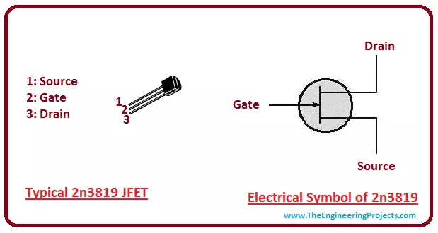
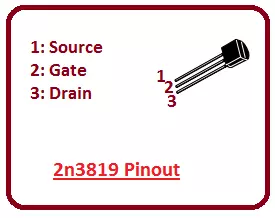
2n3819 Pinout
2n3819 mainly consists of three terminals.
1: Source2: Gate3: Drain
Current will from flow from source to drain.
It is a voltage control device and gate draws no current.
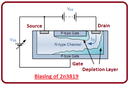
Working of N-Channel 2n3819
There exists a conduction path between source and drain.
The amount of electric charge can be controlled passing through the channel.
By liming the area of channel path we can limit the charge flow from source to drain terminals.
Conduction channel is made using the field effect. When a positive voltage is applied at the gate and source terminals it helps in reverse biasing the gate-source pn-junction, which ultimately enlarges the depletion region.
Following figure shows the P-Type gate is diffused in the N-Type material which forms the reverse biased pn-junction.
This pn-junction will create a depletion region around the gate terminal.
It is called depletion region because no charge carriers exist in this region.
This depletion region will create a potential gradient around the pn-junction, and helps in limiting the flow of current between channel from source to drain by reducing the width of the conduction channel.
N-Channel JFET sometimes referred as depletion mode devices when there is no voltage applied at the gate terminal.
The conduction from source to drain will stop when depletion layer exceeds the width of the conduction channel.
The point at which conduction stops is called pinch off region.
Pinch off value is different for different transistors.
In order to switch off this N-Channel JFET, negative gate-source voltage is required Vgs.
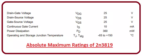
Absolute Maximum Ratings of 2n3819
Absolute maximum rating of 2n3819 is shown in the figure below.
It is important to note that if stresses are exceeded from the given absolute value, they can harm the device.
Also, if stresses are applied for extended period of time above the normal operating conditions, they can effect the device reliability.
Applications
2n3819 is widely used for high frequency amplifier.
It can be used in low capacitance switches.
For general purpose amplification and analog switching we use this N-Channel JFET.
That's all for today. If you have any question or query you can ask me in the comment section below. I'll try my best to help you according to best of my expertise. Your feedback and suggestion will be highly appreciated. They will help us provide you quality work that resonates with your needs and requirements. Stay tuned.
syedzainnasir
I am Syed Zain Nasir, the founder of The Engineering Projects (TEP). I am a
programmer since 2009 before that I just search things, make small projects and now I am sharing my
knowledge through this platform. I also work as a freelancer and did many projects related to
programming and electrical circuitry. My Google Profile+Follow
Get Connected
Comments on ‘’ Introduction to 2n3819 ‘’ ( 1 )
0
testuser
Says:
This part is now obsolete, is there similar quality replacement available?
Reply