


Introduction to ATmega128


Introduction to ATmega128
- ATmega128 is an AVR, 8-bit low power microcontroller that contains 64-pin interface and is based on RISC architecture.
- It is mainly used in an embedded system and industrial automation.
- This AVR controller differs from PIC controllers in accordance with the instruction set where AVR requires one clock cycle to execute a number of instructions while PIC controllers need a number of clock cycles to execute a single instruction.
- The ADC is included in the device that makes it an ideal choice for sensor interfacing where it receives the analog signal and converts it to a digital one. There are total 8 channels available on the ADC module.
- Apart from communications protocols like SPI, I2C, and USRAT, this tiny module comes with watchdog timers, external interrupts, power up timer, 6 sleep modes and programming enable pin.
- The Program Memory is based on Flash and comes with a memory space around 128K while EEPROM and SRAM are 4K each.
- If you are an expert or newbie, you need this module every now and then for the development of the electronic projects where automation is a major concern. Ability to perform a number of functions without buying external components makes this device highly economical and best choice for the tech geeks.
1. ATmega128 Features
This AVR microcontroller comes with very useful features. Large memory space and number of pins make this device a step ahead for driving automation in the relevant project. Following table shows the main features of ATmega128.| No. of Pins | 64 |
| CPU | 8-Bit AVR |
| Operating Voltage | 4.5 to 5.5 V |
| Program Memory | 128K |
| Program Memory Type | Flash |
| RAM | 4K |
| EEPROM | 4K |
| ADC Number of ADC Channels | 10-Bit 8 |
| Analog Comparator | Yes |
| PWM Channels | 6 |
| Oscillator | up to 16 MHz |
| Timer (4) | 16-Bit Timer (2) 8-Bit Timer (2) |
| Packages (3) | PDIP TQFP QFN |
| Power Up Timer | Yes |
| I/O Pins | 53 |
| Manufacturer | Microchip |
| SPI | Yes |
| I2C | Yes |
| Watchdog Timer | Yes |
| Brown out Detection (BOD) | Yes |
| USART | Yes |
| Sleep Modes | 6 |
| Minimum Operating Temperature | -40 C |
| Maximum Operating Temperature | 85 C |
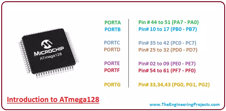
2. ATmega128 Pinout and Pin Description
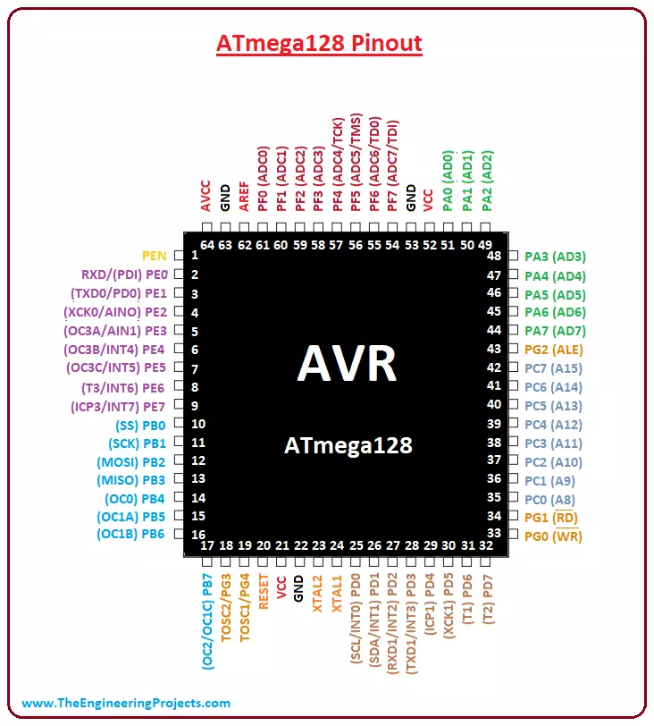
The pinout and pin description of each pin will help you understand the major functions associated with each pin. Some pins are able to perform more than one functions on each pin.Pinout
Following figure shows the pinout of ATmega128.
- The AVCC is the voltage applied to the ADC module while AREF is the reference voltage applied to the controller. The VCC and GND are the voltage supply and ground pins respectively.
Pin Description
Following table shows the description of each pin.| 1 | PEN | Programming Enable |
| 2 | PE0 RXD PDI | I/O Pin Serial Receive Pin (USART) |
| 3 | PE1 TXD PDO | I/O Pin Serial Transmit Pin (USART) |
| 4 | PE2 XCK0 AIN0 | I/O Pin External Interrupt PinAnalog Comparator Positive |
| 5 | PE3 OC3A AIN1 | I/O Pin Dedicated Pin for Timer (PWM Channel) Analog Comparator Negative |
| 6 | PE4 OC3B INT4 | I/O Pin Dedicated Pin for Timer (PWM Channel) Interrupt |
| 7 | PE5 OC3C INT5 | I/O Pin Dedicated Pin for Timer (PWM Channel) Interrupt |
| 8 | PE6 T3 INT6 | I/O Pin Timer 3 Interrupt |
| 9 | PE7 ICP3 INT7 | I/O Pin Timer/Counter3 Input Capture Pin Interrupt |
| 10 | PB0 SS | I/O Pin SS (Slave Select Input for SPI). This pin is set to low when the controller acts as a slave |
| 11 | PB1 SCK | I/O Pin SCK (Serial Clock for SPI). This clock is shared between the controller and external devices for accurate data transfer |
| 12 | PB2 MOSI | I/O Pin MOSI (Master Output Slave Input) for SPI communication. The data is received by this pin when the microcontroller acts as a slave |
| 13 | PB3 MISO | I/O Pin MISO (Master Input Slave Output) for SPI communication. The data is sent to the master using this pin when microcontroller acts as a slave |
| 14 | PB4 OC0 | I/O Pin PWM Channel Output |
| 15 | PB5 OC1A | I/O Pin PWM Channel Output |
| 16 | PB6 OC1B | I/O Pin PWM Channel Output |
| 17 | PB7 OC2 OC1C | I/O Pin PWM Channel Output |
| 18 | PG3 TOSC2 | I/O Pin MISO (Master Input Slave Output) for SPI communication. When the controller acts as a slave, the data is sent by a controller to master through this pin Interrupt |
| 19 | PG4 TOSC1 | I/O Pin SCK (SPI Bus Serial Clock). This clock is shared between the controller and other devices for data transfer Interrupt |
| 20 | RESET | Voltage Supply Pin for ADC |
| 21 | VCC | Voltage Reference |
| 22 | GND | Ground Pin |
| 23 | XTAL2 | Crystal Oscillator Output |
| 24 | XTAL1 | Crystal Oscillator Input |
| 25 | PD0 SCL INT0 | I/O Pin I2C communication External Interrupt 0 |
| 26 | PD1 SDA INT1 | I/O Pin I2C communication External Interrupt 1 |
| 27 | PD2 RXD1 INT2 | I/O Pin Serial Communication Receive Pin (USART) External Interrupt 2 |
| 28 | PD3 TXD1 INT3 | I/O Pin Serial Communication Transmit Pin (USART) External Interrupt 3 |
| 29 | PD4 ICP1 | I/O Pin Timer/Counter1 Input Capture Pin |
| 30 | PD5 XCK1 | I/O Pin External Clock I/O for USART |
| 31 | PD6 T1 | I/O Pin Timer 1 |
| 32 | PD7 T2 | I/O Pin Timer 2 |
| 33 | PG0 WR | I/O Pin Control Pin for writing to the external memory |
| 34 | PG1 RD | I/O Pin Control Pin for reading from the external data memory |
| 35 | PC0 A8 | I/O Pin |
| 36 | PC1 A9 | I/O Pin |
| 37 | PC2 A10 | I/O Pin |
| 38 | PC3 A11 | I/O Pin |
| 39 | PC4 A12 | I/O Pin |
| 40 | PC5 A13 | I/O |
| 41 | PC6 A14 | I/O Pin |
| 42 | PC7 A15 | I/O Pin |
| 43 | PG2 ALE | I/O Pin ALE (Address Latch Enable), it is used when multiple memory chips are connected to the microcontroller and only one of them needs to be selected |
| 44 | PA7 AD7 | I/O Pin |
| 45 | PA6 AD6 | I/O Pin |
| 46 | PA5 AD5 | I/O Pin |
| 47 | PA4 AD4 | I/O Pin |
| 48 | PA3 AD3 | I/O Pin |
| 49 | PA2 AD2 | I/O Pin |
| 50 | PA1 AD1 | I/O Pin |
| 51 | PA0 AD0 | I/O Pin |
| 52 | VCC | Voltage Supply Pin |
| 53 | GND | Ground |
| 54 | PF7 ADC7 TDI | I/O Pin ADC Channel 7 JTAG Interface |
| 55 | PF6 ADC6 TDO | I/O Pin ADC Channel 6 JTAG Interface |
| 56 | PF5 ADC5 TMS | I/O Pin ADC Channel 5 JTAG Interface |
| 57 | PF4 ADC4 TCK | I/O Pin ADC Channel 4 JTAG Interface |
| 58 | PF3 ADC3 | I/O Pin ADC Channel 3 |
| 59 | PF2 ADC2 | I/O Pin ADC Channel 2 |
| 60 | PF1 ADC1 | I/O Pin ADC Channel 1 |
| 61 | PF0 ADC0 | I/O Pin ADC Channel 0 |
| 62 | AREF | Reference Voltage |
| 63 | GND | Ground |
| 64 | AVCC | Voltage Supply Pin for ADC |
3. ATmega128 Main Functions
ATmega128 can perform a number of functions on a single chip. Large memory space with more number of pins interface put this device ahead of other controllers available in the AVR community. Following are the major functions associated to this tiny module.Timer
Atmega128 comes with four timers i.e. two 8-bit and two 16-bit timers. These timers play a vital role in creating a delay of any running functions and can be used both ways i.e. timers as well as counters where former is used to control the internal functions of the controller and increments the instruction cycle, while later counts the number of intervals by incrementing the rising and falling edge of the pin and is mainly used for external functions. Two other timers added in the device are- Oscillator Start-up Timers
- Power Up Timer
Number of Sleep Modes
This device incorporates Six Sleeping Modes for power saving purpose. These modes include:- Power-save
- Power-down
- Idle
- ADC Noise Reduction
- Standby
- Extended Standby
Brown Out Detect (BOD)
The BOD, also known as BOR (Brown Out Reset), is a valuable addition to the device that helps in resetting the module once the Vcc (voltage supply) goes below a brownout threshold voltage. In this mode, multiple voltage ranges are produced to save the module once the power drops at the voltage supply line. If you aim to bring back the device from BOD function, it is advised to enable the Power Up Timer for creating a slight delay.Watchdog Timer
Most of the chips, if not all, produced by Microchip, incorporate a built-in watchdog timer that resets the controller if the running program hangs up during compilation or gets stuck in the infinite loop. The main purpose of this timer is to prevent the controller from resetting it manually, giving you a slight edge over other processors where you need to wrestle your mind to manually reset the controller in case there comes a glitch in the running function. The watchdog timer behaves like a countdown timer.Interrupt
The interrupts are very helpful for calling the desired function that puts the main running function on hold until the required instruction is executed. The controller goes back to the main program once the interrupt is executed.I2C Communication
I2C protocol is used to layout the communication between low-speed devices like ADC and DAC converters and microcontrollers. It is a two wire communication that mainly contains two lines- Serial Clock (SCL)
- Serial Data (SDA)
SPI Communication
ATmega128 houses a serial peripheral interface (SPI) that is mainly used for communication between the microcontroller and other peripheral devices such as sensors, shift registers, and SD cards. Separate clock and data lines are available, layered with a select line for selecting the relevant device for communication. Two pins used for SPI communication are as follow- MOSI (Master Output Slave Input)
- MISO (Master Input Slave Output)
4. ATmega128 Compilers
Compilers are the basic software used for writing and compiling the code into the AVR controller. Some are free to use and some are paid. If you are getting your hands-on very first time with the controllers, it is advised to go with the free version, you can move to paid version as you grow and learn with the passage of time. Following are some basic compilers mainly used for AVR microcontrollers.- The IAR is a paid compiler and comes with a professional interface. As per the testimonials and personal experience of some of the experts, this compiler proves to the best version for the AVR microcontrollers.
- CodeVision houses a CodeWizard and turns out to be highly economical for the controllers.
- The GCC Port is another good pick to start with, but it comes with a bit complex interface. It works with both Windows and Linux operating systems.
- ImageCraft is a valuable addition for compiling the code, but it doesn't incorporate some GUI features like editor and project management that may put you in big trouble during the code execution.
5. ATmega128 Memory Interface
Two memory types are mainly used in ATmeag128 named as Program Memory (Flash Memory) and SRAM memory where former makes use of a single pipelining for the execution of the instructions and later is a volatile memory mainly depends on the power supply source. This AVR module incorporates a Harvard Architecture where separate memories spaces are reserved for both data and program. The memory space in the controller is nothing but a combination of the linear and regular memory maps. The Fast Access File Register is layered with 32 x 8 – Bit general purpose working registers. The single clock cycle is enough for accessing these registers and laying out the ALU (Arithmetic Logic Unit) operation where the result is stored in the Register file.Program Memory (ROM)
Program memory has a memory space around 128K where recent instruction is called followed by the next instruction, executing the instructions in every clock cycle.- It is mainly categorized into two parts named as the Boot Program section and Application Program section. The former comes with Applications Flash Memory that plays the main part for SPM instruction writing.
Data Memory (RAM)
The data memory has a memory space around 4K. Five different addressing modes in the AVR architecture are used for addressing this RAM memory. These modes are named as- Direct
- Indirect
- Indirect with Displacement
- Indirect with Pre-decrement
- Indirect with Post-increment.
- The ALU module operates in a single clock cycle and is divided into three main functions called direct, arithmetic and bit functions, that are directly connected with 32 general purpose registers.
6. ATmega128 Block Diagram
Following figure shows the block diagram of ATmega128.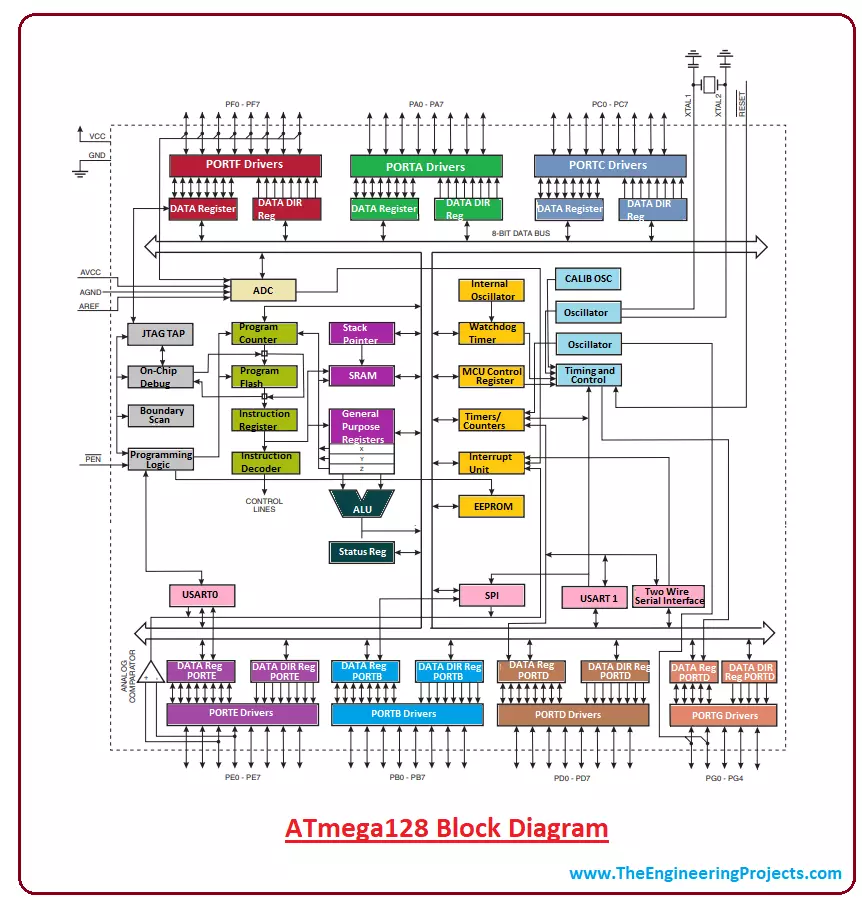
- ATmega128 comes with six software selectable power saving modes. The Power-down is very helpful for freezing the Oscillator and stops all other module functions while keeping the register contents saved. The functions remain disabled until the next interrupt is called and executed.
- Similarly, the Idle mode allows the interrupt system, SPI Port, SRAM, Timers/Counter to function while keeping the CPU disabled.
- The ADC Noise Reduction mode plays a vital role in minimizing the switching noise and freezes entire module except asynchronous ADC and Timers.
- In the Power-save mode, the entire device is sleeping except asynchronous timer which continues to run.
- The Standby mode puts the whole device in sleep mode except Crystal Oscialltor which continues to run, helping to consume low power. The Extended Standby mode allows both the Oscillator and the Asynchronous Timer to run while the rest of the device sleeps.
ATmega128 Applications
- Embedded systems
- Industrial Automation
- Students Projects
- Making of quadcopters
- Home automation
×
![]()


