


- Phase detector operates with the aim to adjust the two signal and make them quite in line with each other so they generate signals with the same magnitude.
Introduction to CD4046
CD4046 is a Micropower Phase-Locked Loop (PLL) that comes with a phase detector for comparing the phase of the output signal with the input signal and adjust them in order to make the matching signals from both ends.- It comes with a common comparator input and a common signal input amplifier between a low-power linear voltage-controlled oscillator (VCO) and two different phase comparators.
- The VCO (Voltage Controlled Oscillator) is an integral part of the IC that mainly generates oscillated frequency based on the applied input. The generated frequency is then used for phase modulation.
- It is important to note that both signal input and comparator input are set at 50% duty cycle where Phase Comparator I can lock the input frequencies that match with the magnitude of the VCO center frequency.
CD4046 Features
Following table shows the main features of CD4046.| Number of Pins | 16 |
| Min Supply Voltage | 3 V |
| Max Supply Voltage | 18 V |
| Number of Phase Comparators | 2 |
| VCO linearity | 1% |
| Power consumption | 70 µW at VCO Frequency= 10 kHz and VDD = 5 V |
| Technology | CMOS Phase Locked Loop |
| Operating Temperature Range | -55 to 125 ºC |
- These ratings will help you make a final decision before you intend to incorporate this device into the relevant project.
CD4046 Pinout
Following figure shows the pinout of CD4046.
- VSS represents the ground voltage while VDD represents the supply voltage.
- A 5.2-V Zener diode is added with the aim to supply regulation if required.
CD4046 Pin Configuration
Following table shows the pin configuration of each pin.| Pin# | Pin Name | Pin Description |
|---|---|---|
| 1 | Phase Pulse | Phase pulse applied to the IC |
| 2 | Phase Comp I Out | An output of Phase Comparator I |
| 3 | Comparator IN | Input at the Comparator |
| 4 | VCO OUT | Output Signal at VCO |
| 5 | INHIBIT | Allows to electronically turn on or off the output voltage power supply |
| 6 | C1A | Capacitor 1 connected to VCO |
| 7 | C1B | Capacitor 2 connected to VCO |
| 8 | VSS | Ground Pin |
| 9 | VCO IN | Input Signal at VCO |
| 10 | Demodulator OUT | Extracting the original signal |
| 11 | R1 | Resistor 1 connected between VCO and Supply Voltage |
| 12 | R2 | Resistor 2 connected between VCO and Supply Voltage |
| 13 | Phase Comp II OUT | Generated oscillated output at Phase II Comparator |
| 14 | Signal IN | Input Signal applied to the Phase Comparator I |
| 15 | Zener | 5.2 V Zener diode for voltage regulation |
| 16 | VDD | Voltage supply pin |
- I hope this configuration will help you understand the major functions associated with each pin on the chip.
Absolute Maximum Ratings
Following figure shows the absolute maximum ratings of CD4046.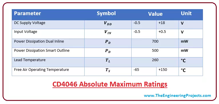
- These are the stress ratings above which the device may stop working. Before you start your project, make sure your technical requirements match with the ratings of the device otherwise it may cause more damage than good.
- As mentioned above DC supply voltage ranges between -0.5 to 18, however it is advised to keep the DC supply between 3 to 15 V for better results, similarly recommended operating temperature range lies from -55 to 125 ºC.
- The ground voltage is zero unless specifically recommended by the manufacturer.
CD4046 Dimensions
Following figure shows the dimension of CD4046.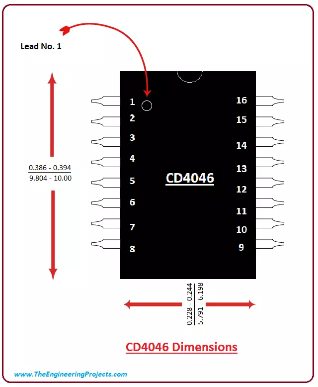
- The dimensions in the numerator are given in inches and dimensions appearing in the denominator are given in millimeters.
- It is a low weight tiny chip that can easily stand fit in the hard to reach places.
Applications
CD4046 comes with a variety of applications aiming to compare the output signals with the input signals and produce them with the same frequencies. Following are the major applications of CD4047.- FSK modulation
- Voltage-to-frequency conversion
- Motor speed control
- FM demodulator and modulator
- Frequency discrimination
- Frequency synthesis and multiplication
- Tone decoding
- Data synchronization and conditioning
