Introduction to 2n5415

Introduction to 2n5415
2n5415 is a PNP transistor that is mainly used for general purpose low-power amplifying and switching applications.- It operates on a general amplification principle where small current at one terminal is used to control large current at other two terminals.
- These terminals are different in terms of doping concentration and size where a base is lightly doped and is responsible for the transistor action as it controls the number of holes flowing from emitter to collector.

- The collector terminal is moderately doped and comes in a bigger size as compared to the other two terminals. It is mainly used to collect the holes emitted from the base terminal.
- The base terminal voltage has a large influence on the output current obtained at the collector terminal. This process is used for amplification purpose.
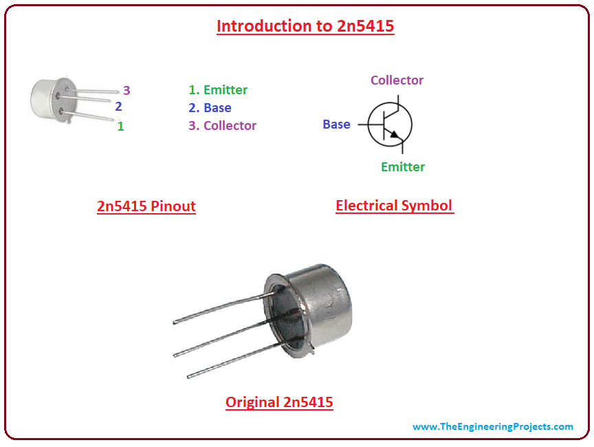
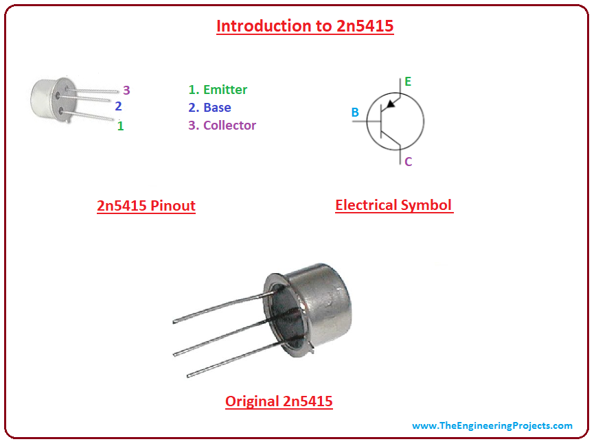
2n5415 Pinout
Following figure shows the pinout of 2n5415.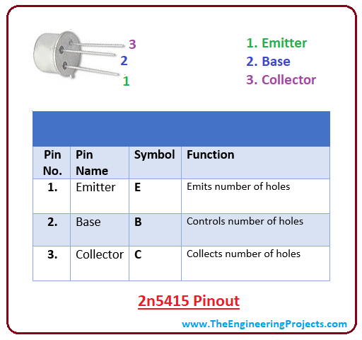
- Holes control the conductivity in this PNP transistor similar to electrons that control the conductivity in NPN transistors.
- In PNP transistor base is more negative as compared to emitter and collector.
2n5415 Circuit Diagram
Following figure shows the circuit diagram of 2n5415.- As mentioned earlier, the emitter terminal is highly doped and comes with 100% transistor current i.e. emitter current is a sum of current at collector and base terminals.
- When the voltage is applied, holes are diffused through the base from the emitter in this PNP transistor which eventually collected by the collector.
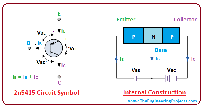
- Most of the professionals prefer NPN transistor over PNP transistor for amplification purpose because they consider conduction carried out by the movement of electrons is more effective and suitable than conduction carried out by the movement of holes.
2n5415 Absolute Maximum Ratings
Following figure shows the absolute maximum ratings of 2n5415.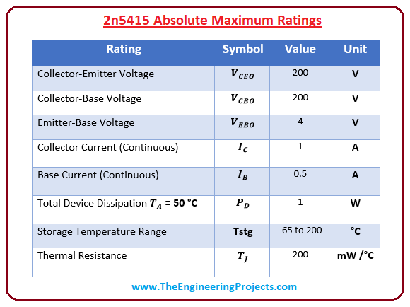
- These are the stress ratings which directly affect the execution of electronic circuit. If these stress ratings are exceeded from absolute maximum ratings, they can damage the device at large, ultimately affecting the overall nature and performance of the project.
- It is preferred to examine these ratings before placing the device in the circuit and make sure the device follows the same stress ratings as defined by the manufacturer.
Applications
- It is widely used in general purpose low-power amplifying circuits.
- Many switching applications are incorporated with this transistor.
×
![]()


