


Introduction to PN2222


Introduction to PN2222
- The PN2222 is a conjoint NPN bipolar junction transistor which is used for common persistence less power intensifying or swapping circuits applications.
- The PN2222 was a fragment of an intimate of expedients designated by Motorola at a 1962 IRE treaty. Meanwhile, then it has been prepared by many semiconductor corporations, such as Texas Instruments.
- PN2222 is an NPN transistor the pinout of emitter and collector will be uncluttered when we attach base pin with the ground and these pins will be fastened when a signal is delivered on base.
- It's gain value is 110 to 800, this value governs the intensification capability of the transistor.
- The maximum quantity of current that can drift by the Collector pin is 800mA, hereafter we cannot attach loads which devour more than 800mA by this transistor.
- For biasing of transistor we must apply current to base pin. This (Ib) current must be limited to 5mA.
-
When this transistor is completely biased then it can permit a maximum of 800mA to movement crosswise the collector and emitter.
-
This phase is named Saturation Region and the characteristic voltage permissible crossways the Collector-Emitter (VCE) or Base-Emitter (VBE) can be 200 and 900 mV correspondingly.
-
When the base current is detached the transistor converts entirely off, this phase is named as the Cut-off Region and the Base-Emitter voltage might be about 660mV.
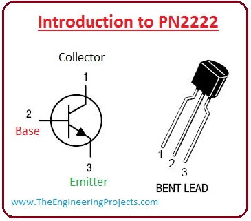
Pinout of PN2222
-
- These are the main pinout of PN2222.
| Pin# | Type | Parameters |
| Pin#1 | Emitter | Emitter is for current drainage out. |
| Pin#2 | Base | The base controls the biasing of the transistor. |
| Pin#3 | Collector | The emitter is for the current inward movement. |

Features of PN2222
- These are the main specifications of PN2222.
- It is bi-polar higher current user NPN transistor.
- It DC gain is (hFE ) is 100.
- Its incessant Collector current (IC) is 800mA.
- Its (VBE) Emitter-base voltage is six volts.
- Its voltage between collector and emitter is thirty volts.
- Extreme base current Ib is 5mA.
- It's accessible in To-92 Compendium.
- Its collector intemperance factor is 0.625 W.
- Its changeover frequency is 300 MHz.
- It has a functioning and storing connection temperature range -55 to +150 °C.
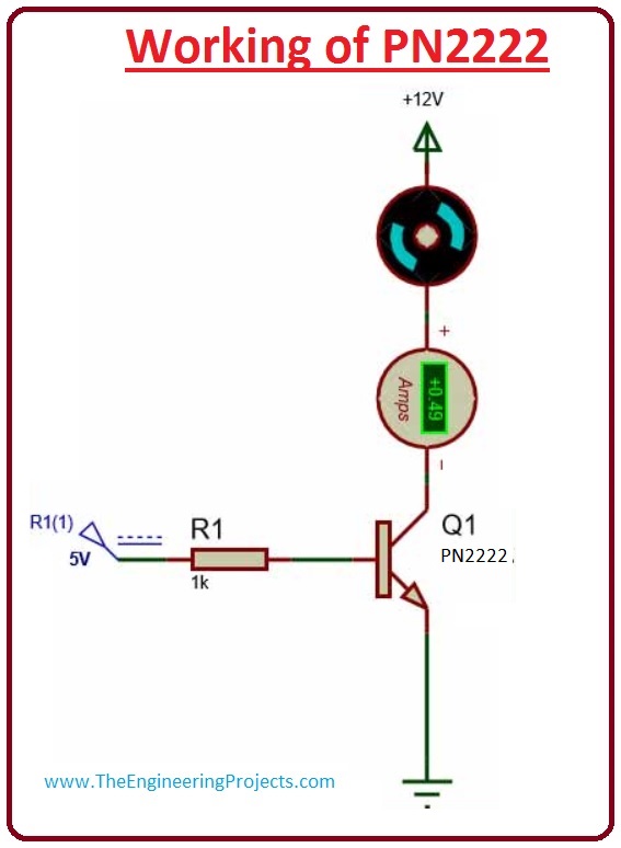
Working of PN2222
- Now we discuss the working of PN2222.
- In the next few lines, we will discuss where it can be used after this we discuss it's working.
- It is like the generally used NPN transistor BC547. Nevertheless, there are two significant topographies which differentiate both of them.
- It can permit collector current up to 800mA and as well has power intemperance of 652mW due to this it is used for larger loads then BC547.
- So if you are considering for an NPN transistor which can switch loads of large current user then PN2222 will be the right option for your industrial developments.
- Now, we discuss its working.
- Like other transistors, it can be used as an amplifier and switch. Voltage crossways of base and emitter are six volts so we have to apply these voltage crossways base and emitter to persuade a base current of the transistor.
- This will change it to forward biasing and consequently completions the linking amid collector and emitter.
- One important thing in this circuit is the base resistor which is a current preventive resistor. This resistor in the circuit is for limit the coming current which can damage the transistor. Its value can be found by the given equation.
- RB = VBE / IB
- To mark things modest I have exposed a basic circuit of the transistor as a switch. In a real circuit, alterations must be vital. In this circuit, I supplied five volts to base and 1K resistor to limit the current.
- Notice that in this circuit motor consumes around 500mA by the 12V supply source, meanwhile PN2222 rating of collector up to 800mA, which shows it's importance that if we have BC547 in the circuit it would be damaged.

Applications of PN2222
- These are some applications of PN2222.
- It is used where higher current consumer loads in the circuit. It also used in numerous swapping submissions.
- It used to control the speed of different types of motors.
- It used in inversion and rectification circuits.
- It also used in Darlington pairs.
×
![]()


