Introduction to BD135

Introduction to BD135
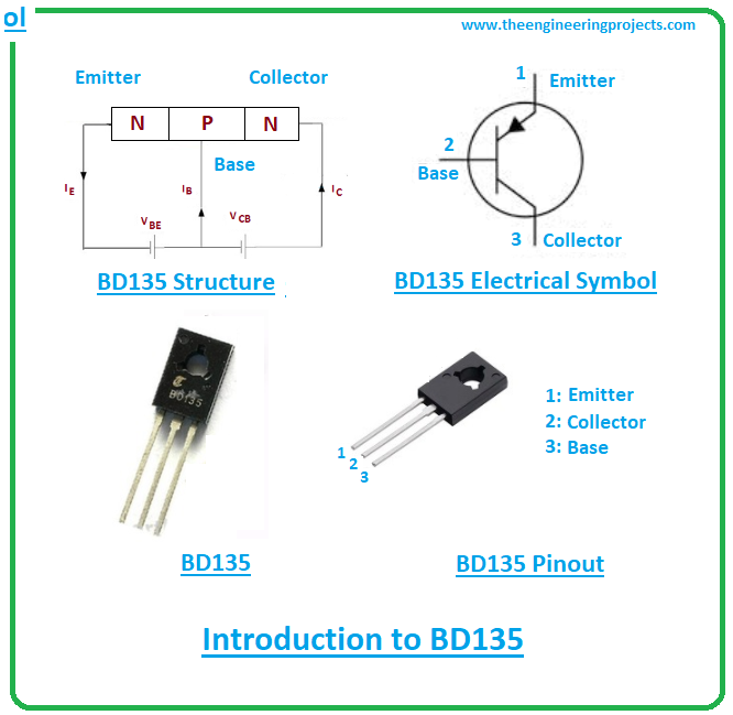
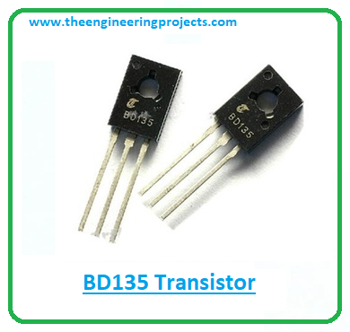
- BD135 is an NPN transistor made-up of silicon material. It is a medium power transistor mainly used for audio amplification and switching purpose.
- This NPN transistor comes with three terminals called emitter, base, and collector. Where small current at the base side is used to produce large current at the other two terminals. This process is used for amplification purposes.
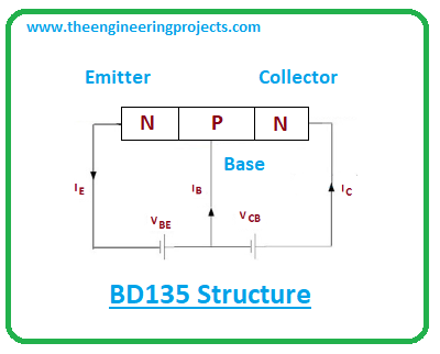
- BD135 carries three layers where one is a p-doped layer and the other two are n-doped layers. The p-doped layer stands between the two n-doped layers.
- In this transistor, the base terminal is positive and represents the p-doped layer while the other two terminals are negative.
- It is important to notice that both electrons and holes play a vital role in conductivity. As this is an NPN transistor, here electrons are majority carriers in opposed to PNP transistors where holes are majority carriers.
- In both cases, however, the base terminal plays the key role to control the overall transistor action.
- In NPN transistor, the base pin controls the number of electrons emitted from the emitter side, and in PNP transistor this base terminal controls the number of holes emitted by emitter which are then collector by the collector side.
BD135 Datasheet
Before employing this component into your electrical projects, it is wise to have a look at its datasheet that will help you get a hold of the main characteristics this element holds. Click below to download the datasheet of the BD135 transistor.BD135 Pinout
BD135 carries three terminals called: 1: Emitter 2: Collector 3: Base The following figure shows the pinout of the BD135.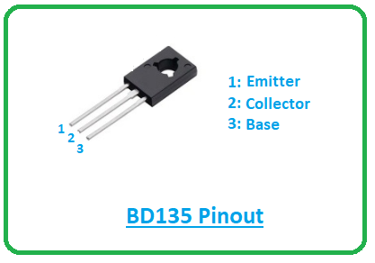
BD135 Pin Configuration
BD135 transistor is available in the following three configurations: 1: Common emitter configuration 2: Common collector configuration 3: Common base configuration- Common emitter configuration is used for amplification purposes as it comes with the suitable voltage and current ratings required for amplification.
- The amplification factor or current gain is an important factor of the transistor that demonstrates the capacity of any transistor it can amplify the current. It is a ratio between collector current and base current and is denoted by ß. In this case, the amplification factor ranges from 40 to 250. As this is a ratio between the same element i.e. current it carries no unit.
- The current gain is another important factor that is mainly used to demonstrate the nature of the transistor. It is known as alpha and is denoted by a. It is a ratio between collector current and emitter current. The alpha value is always less than 1, commonly lies from 0.5 to 1.
BD135 Working Principle
- Recall, the base pin is responsible for the overall transistor action. This pin behaves like an electron valve that controls the number of electrons emitted from the emitter terminal.
- The base terminal behaves similarly in the PNP transistor but here it controls the number of holes.
- The small current at the base terminal is amplified and produced across the other terminals during the amplification process.
- And when BD135 behaves like a switch, it changes the small current present at one side of the transistor into a larger current across the remaining terminals.
- As BD135 is an NPN transistor, here the base pin is positive with respect to the emitter terminal and the collector voltage is more positive than the emitter voltage.
- Also, the collector side is connected with the resistor to limit and control the flow of current.
BD135 Power Ratings
The following table shows the absolute maximum ratings of BD135.| Absolute Maximum Ratings BD135 | ||||
|---|---|---|---|---|
| No. | Rating | Symbol | Value | Unit |
| 1 | Collector-Emitter Voltage | Vce | 45 | V |
| 2 | Collector-Base Voltage | Vcb | 45 | V |
| 3 | Emitter-Base Voltage | Veb | 5 | V |
| 4 | Collector Current | Ic | 1.5 | A |
| 5 | Current Gain | hfe | 40 to 250 | |
| 6 | Power Dissipation | Ptot | 12.5 | W |
| 7 | Storage Temperature | Tstg | -55 to 150 | C |
- These are the stress ratings. Make sure ratings don’t exceed the absolute maximum ratings, else they can damage the component and thus the entire project.
- Also, if these ratings are applied for more than the required time, they can severely affect device reliability.
BD135 Alternatives
The following are the alternatives to BD135.- BD131
- BD135G
- BD167
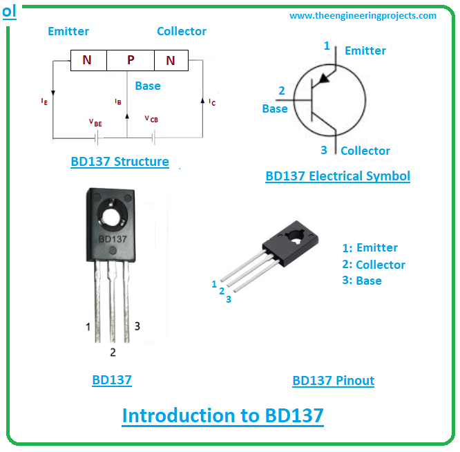
- BD137
- BD139G
- BD169
- BD137G
- BD139
- BD165
- It is important to note that… before employing these components in your electrical circuit, check the pinout of the alternatives, as it is likely the pinout of the alternatives differ from the pinout of the BD135. Early due diligence can help you avoid hassle later.
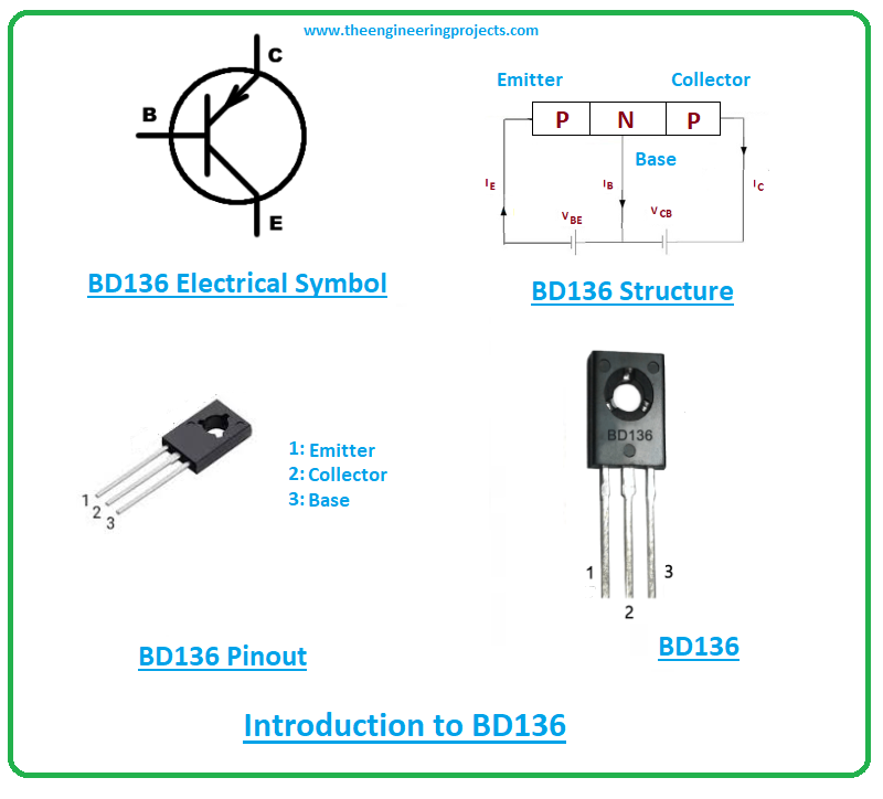
- BD136 is a complementary PNP transistor to BD135.
BD135 Applications
BD135 is used in the following applications.- Used for amplification and switching purposes.
- Used in Astable and Bistable multivibrators.
- Used in sensor circuits.
- Used to control motor.
- Employed in H-bridge circuits
- Used in an audio preamplifier and amplifier stages.
- Used to drive loads under 1.5A.
- Employed in battery chargers.
BD135 Physical dimensions
The following figure shows the physical dimensions of the BD135 transistor.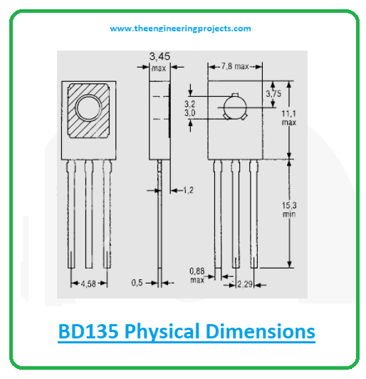
×
![]()


