Introduction to BD137

Introduction to BD137
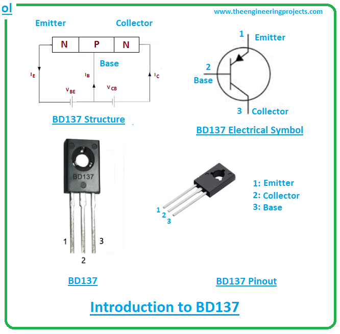
- BD137 is a medium power transistor that falls under the category of NPN transistors.
- It contains three terminals known as emitter, collector, and base. The small input current at the base pin is utilized to create a large current at the other two terminals.
- BD137 is composed of three layers where one p-doped layer sits between the two n-doped layers. The single p-doped layer represents the base terminal which is positive and the other two terminals represent emitter and collector that are negative.
- As this is an NPN transistor, here current flows from the collector pin to emitter pin while the base terminal controls the number of electrons emitted from the emitter pin which are then collected by the collector pin.
- Though both holes and electrons play a vital role in conductivity, here in this NPN transistor, holes are minority carriers while on the other hand electrons are majority carriers.
- This is opposite in the case of PNP transistors where electrons are minority carriers and holes are majority carriers.
- It is important to note that the NPN transistors are widely used for amplification purposes and are preferred over PNP transistors because the movement of electrons is better than the movement of holes.
BD137 datasheet
While incorporating this NPN transistor into your electrical project, it is better to scan through the datasheet of this component that will help you get a better understanding of the characteristics of the component. To download the datasheet of BD137, click the link below.BD137 Pinout
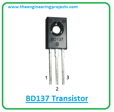
BD137 contains three terminals named 1: Emitter 2: Collector 3: Base The following figure shows the pinout of the BD137 transistor.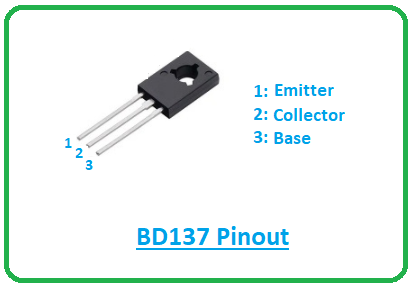
- These pins are used for the connection with the external circuit. All these terminals carry different doping concentrations and different functionality.
- The collector and base pins are less doped as compared to the emitter pin. Plus, the emitter terminal holds the entire current of the transistor.
Pin Configurations
BD137 is used with three main configurations. 1: Common-base configuration 2: Common-collector configuration 3: Common-emitter configuration- The Common-emitter configuration is employed for the amplification purposes because it comes with the exact current and voltage required for the amplification.
- The amplification factor is an important factor of this transistor that defines the capability of the transistor it can amplify the input signal that is then produced as output across the other terminals. It is called beta and is denoted by ß. It is a ratio between the collector current and base current.
- The current gain is another important factor that defines the nature of the transistor. It is denoted by a and is known as alpha. It is a ratio between collector current and emitter current. The alpha value is always less than 1, mostly ranges from 0.5 to 1.
BD137 Working Principle
- No matter the transistor is… whether it’s NPN or PNP transistor, the base pin is used to trigger the overall transistor action.
- This base pin controls the number of electrons in the case of NPN transistor while it controls the number of holes in the case of PNP transistor. This base terminal acts as a control valve.
- In this BD137 NPN transistor, here the base terminal is positive with respect to the emitter side and the emitter voltage is less positive than the collector voltage.
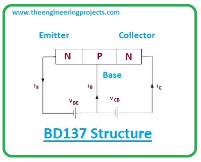
- The small input current at the base side is amplified and created across the remaining two terminals during the amplification process.
- And BD137 also acts like a switch, where it changes the small current available at one side of the transistor into much larger current across the other two terminals.
- Plus, the collector side is coupled with the resistor to control and limit the flow of current.
BD137 Power Ratings
The following table shows the absolute maximum ratings of the component BD137.| Absolute Maximum Ratings BD137 | ||||
|---|---|---|---|---|
| No. | Rating | Symbol | Value | Unit |
| 1 | Collector-Emitter Voltage | Vce | 45 | V |
| 2 | Collector-Base Voltage | Vcb | 45 | V |
| 3 | Emitter-Base Voltage | Veb | 5 | V |
| 4 | Collector Current | Ic | 1.5 | A |
| 5 | Current Gain | hfe | 40 to 250 | |
| 6 | Power Dissipation | Ptot | 12.5 | W |
| 7 | Storage Temperature | Tstg | -55 to 150 | C |
- The emitter-base voltage is 5V which means it needs only 5V to bias the transistor while collector-base and collector-emitter voltages are 45V.
- Power dissipation is 12.5W which projects that it releases 12.5W energy during the working of this transistor. The DC current gain ranges from 40 to 250 which demonstrates the amount of current it can amplify.
- These are main called stress ratings. Make sure while working with your electrical project these ratings don't surpass the absolute maximum rating or they can badly damage the component.
- Moreover, if these ratings are applied for a maximum period, they can affect device reliability.
BD137 Alternatives
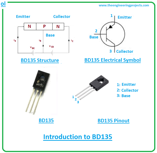
- The BD135 & BD139 are the alternatives to BD137.
- While working with the alternatives, double-check the pinout of the alternatives before using them in your project, as it's quite likely the pinout of the BD137 may differ from the pinout of the alternatives.
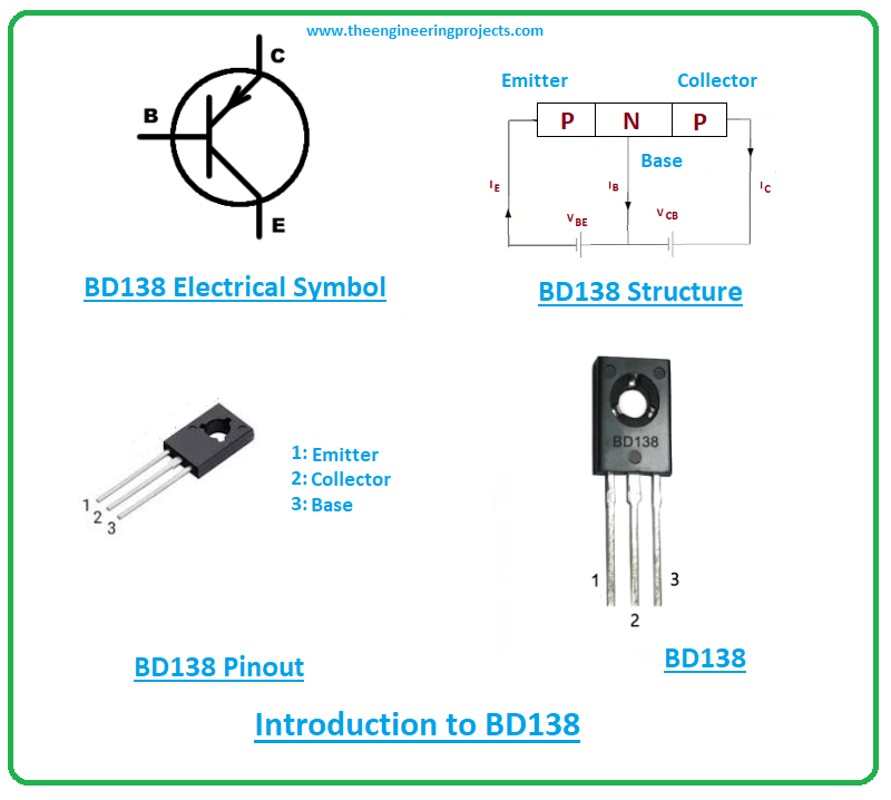
- The complementary PNP transistor to BD137 is BD138.
Applications
BD137 is used in the following applications.- Used to design audio amplifiers and drivers using complementary circuits.
- Used to control motor.
- Employed in an audio preamplifier and amplifier stages.
- Used to support loads under 1.5A.
- Employed in H-bridge circuits.
- Incorporated in battery chargers.
BD137 physical dimensions
The following figure shows the physical dimensions of the BD137 transistor.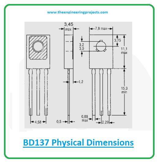
×
![]()


