


KA3525A PWM Controller Datasheet, Pinout, Features & Applications


Hi Everyone! I welcome you on board. Happy to see you around. In this post today, I’ll walk you through the Introduction to KA3525A.
The KA3525A is a monolithic IC chip that features the control circuitry mainly required for a pulse width modulating regulator. This device comes with an error amplifier, voltage reference, pulse width modulator, an under-voltage lockout, an oscillator, the output driver, and a soft start circuit, all in one package.
I suggest you buckle up as I’m going to discuss the complete introduction to KA3525A covering datasheet, pinout, features, and applications. Let’s jump right in.
Introduction to KA3525A
- The KA3525A is a monolithic IC chip that incorporates the control circuitry used for pulse width modulation.
- During the PWM process, the control circuit inside the chip generates variable-width pulses against the amplitude of the input analog signal.
- The PWM is a technique that reduces the power produced by the electrical signal by converting it into discrete several parts. Thus, controlling the value of current or voltage by the switch. This switch is located between the supply & load and controls the value of the input signal when we turn it ON and OFF at a fast rate.

- The term duty cycle is associated with this PWM which is defined as the proportion of ON time of the entire input signal. If the signal remains 10% ON and 90% OFF, then the duty cycle tends to be 10%. If the signal remains 50% OFF and 50% ON, then the duty cycle is said to be 50%.

- This is a 16-pin chip that requires a supply voltage of around 40V and features a reference output current of around 50mA.
- The operating temperature ranges from 0 to 70 C while the storage temperature ranges from -65 to 150 C.
- Power dissipation is 100mW and the output sink current is 500mA.
- This pulse-width modulation regulator IC incorporates 16 pins.
- This device generates two PWM signals that are a complement to each other.
- This component is widely used in switch-mode power supply and other electronic circuits.
- The output voltage is controlled by feedback circuitry that does it by comparing the feedback signal with a reference voltage.
- This device features a shutdown protection circuit that turns off the PWM signal if the feedback signal reaches its limit.

KA3525A Datasheet
Before you use this device in your electrical project, it’s better to go through the datasheet of the device that features the main characteristics of the component. Click the link below to download the datasheet of KA3525A.
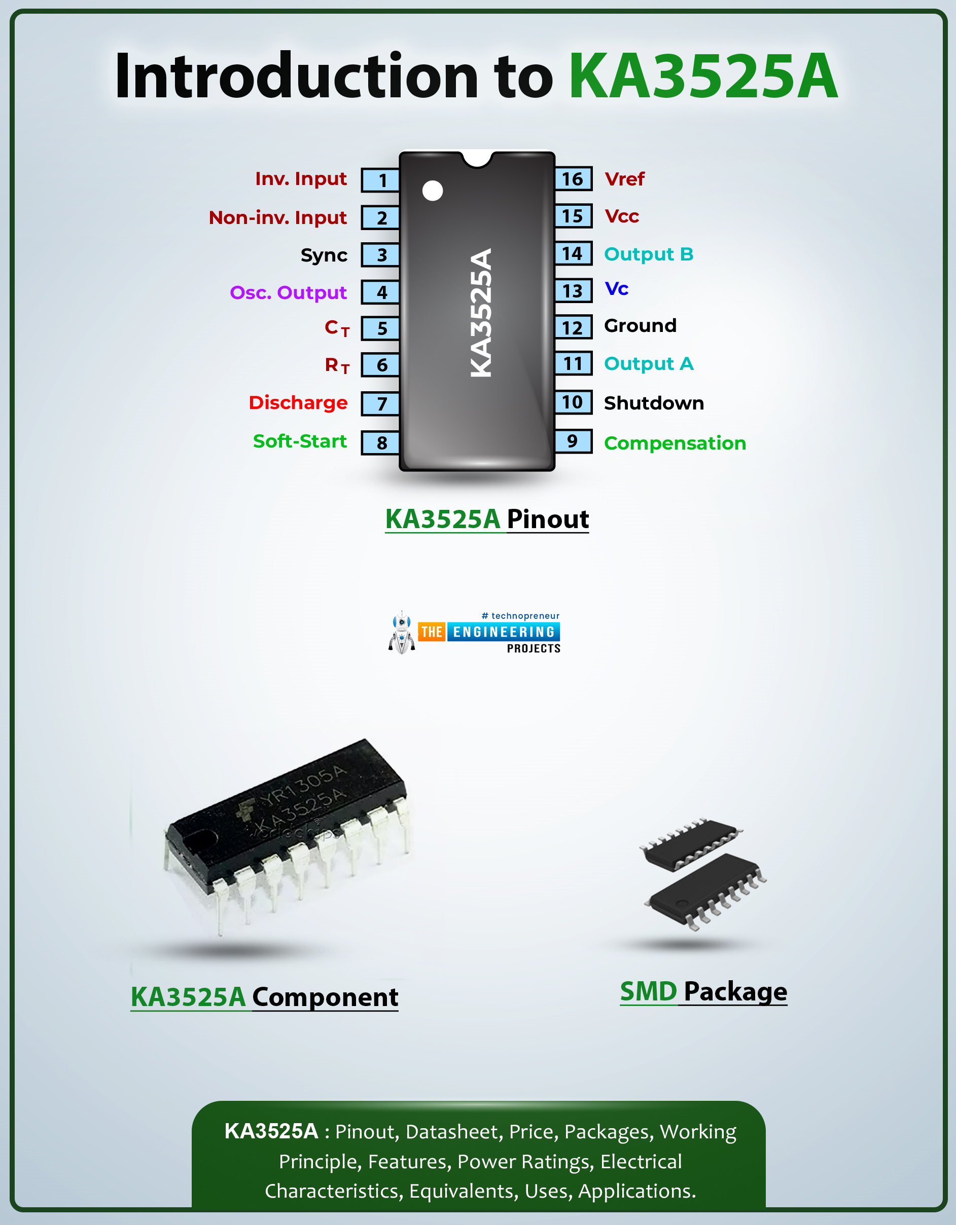
KA3525A Pinout
The following figure shows the pinout diagram of KA3525A.

- Pin 1 represents the inverting pin and pin 2 represents a non-inverting pin.
- If the voltage on the non-inverting pin is less than the voltage on the inverting pin, then the respective duty cycle increases.
- Pin 3 is employed for the synchronization of two waves while Pin 4 is the output pin of an oscillator.
- Pins 5, 6 & 7 are incorporated to adjust the frequency of PWM.
- We can control the frequency of PWM by controlling the value of the discharge resistor, CT capacitor, and RT resistor.
- Pin 8 SS is a soft start pin that enables the output signal after some time. The value of capacitance is directly related to the soft-start time.
- Pin 9 is called a compensation pin employed to prevent rapid fluctuations in the output voltage signal.
- Pin 10 is known as a shutdown pin. It shuts down the PWM signal when the current reaches its limit.
- Pins 11 and 14 are known as the output pins used to provide input to the MOSFETs. KA3525A incorporates a built-in MOSFET driver circuit.
- Pin 13 and 15 are called the power pins. Vc should range from 5-35 volts while Vin should stand between 8-35 volts.
- Pin 16 is known as the reference pin used to adjust the reference voltage through pin 1 or 2.
KA3525A Features
The following are the main features of KA3525A.
- Carries under-voltage lockout.
- Available with Oscillator Sync Terminal.
- Comes with 5V ± 1% Reference.
- Comes with Deadtime Control.
- Features Internal Soft Start.
KA3525A Applications
- It is employed in consumer power electronics applications such as pure sine wave inverters.
- Used to generate a regulated voltage in a boost converter and a buck converter.
That’s all for today. I hope you enjoyed reading this post. If you have any questions, you can pop your query in the section below, I’d love to assist you the best way I can. You’re most welcome to share your valuable suggestions and feedback about the content we share so we keep sharing quality content customized to your exact needs and requirements. Thank you for reading the article.


