


TDA1554 Audio Amplifier Datasheet, Pinout, Features & Applications


Hi Guys! Hope you’re well today. I welcome you on board. In this post today, I’ll walk you through the Introduction to TDA1554.
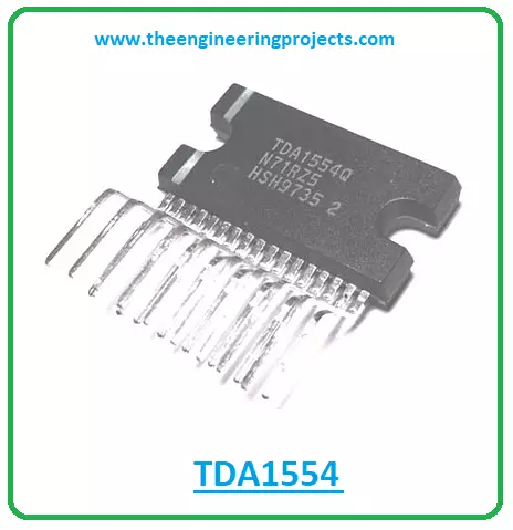
The TDA1554Q is an integrated class-B output amplifier mainly used for car radio applications. This device features 4 x 11 W single-ended or 2 x 22 W bridge amplifiers. It comes in a 17-lead single-in-line (SIL) plastic power package.
I suggest you buckle up and read this entire post till the end as I’ll discuss the complete Introduction to TDA1554 covering datasheet, pinout, features, and applications. Let’s get started.
Introduction to TDA1554
- TDA1554 is a 4*11W single-ended or 2*22W power amplifier IC which means the internal circuitry features a 4*11W single-ended or 2*22W bridge amplifier.
- It is an integrated class-B output amplifier that comes in a 17-lead single-in-line (SIL) plastic power package mainly used for car radio applications.
- Out of four amplifiers incorporated in the device, two are non-inverting and two are inverting amplifiers.
- Moreover, each amplifier comes with a gain of 20dB (26dB in BTL).
- These amplifiers carry low thermal resistance and are thermally protected.
- This device generates high output power and fixed gain.
- Plus, a mute or standby switch is incorporated with the device helping you mute the amplifiers anytime you want.
- This device can handle high energy on outputs and low voltage offsets at outputs and comes with good ripple rejection.
TDA1554 Datasheet
Before you apply this device to your electrical project, it’s better to scan through the datasheet of the component that features the main characteristics of the component. You can download the datasheet of TDA1554 by clicking the link below.TDA1554 Pinout
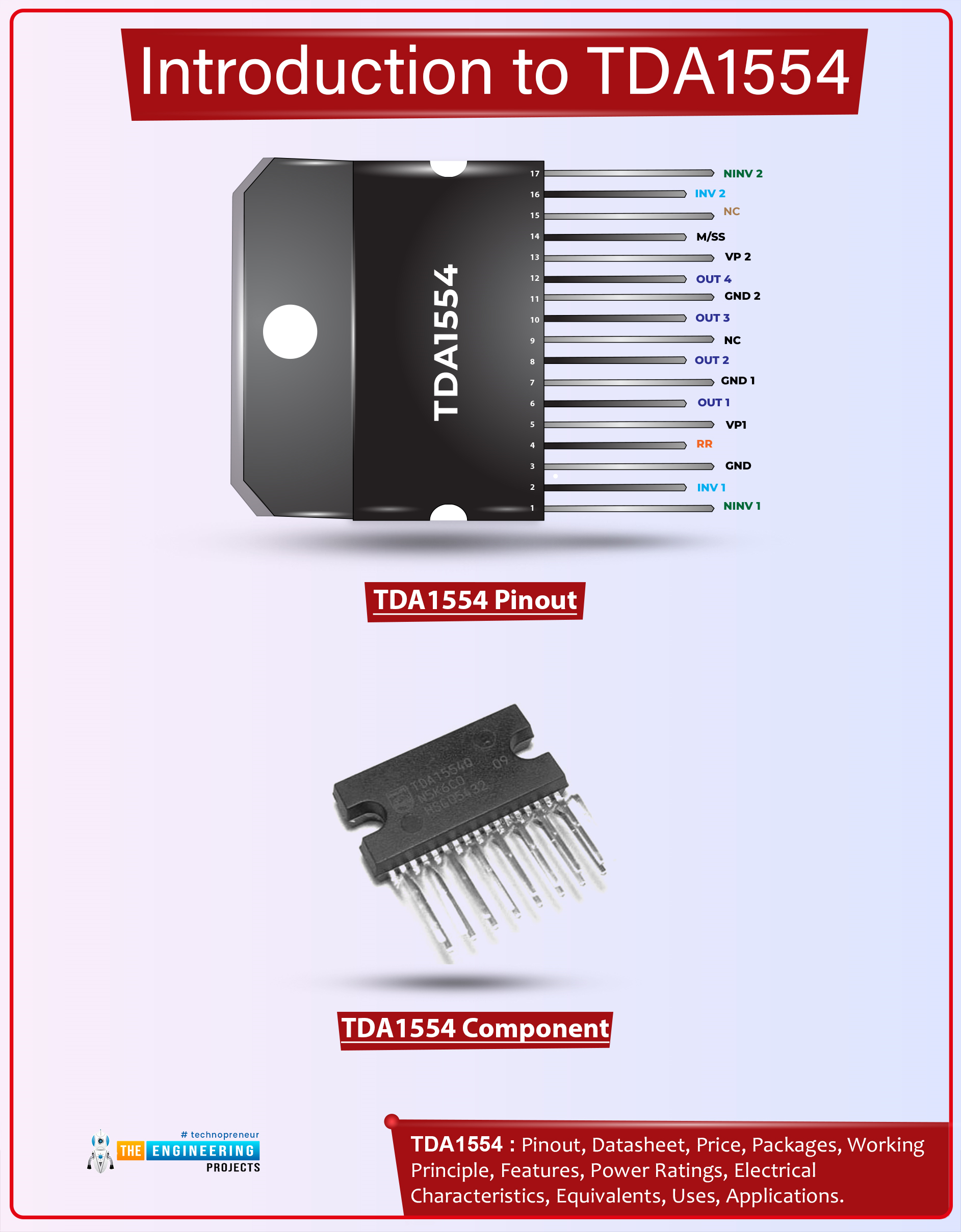
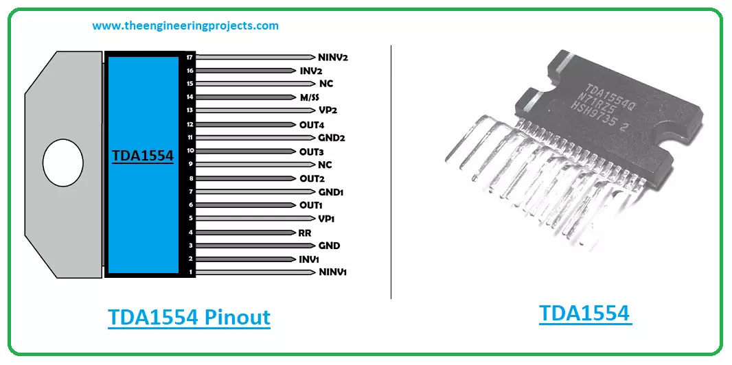
The following figure shows the pinout diagram of TDA1554.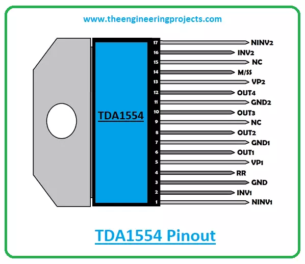
| Pin Description of TDA1554 | ||||
|---|---|---|---|---|
| Pin No. | Pin Description | Pin Name | ||
| 1 | Non-inverting input 1 | NINV1 | ||
| 2 | Inverting input 1 | INV1 | ||
| 3 | Ground (signal) | GND | ||
| 4 | Supply voltage ripple rejection | RR | ||
| 5 | Positive Input Voltage 1 | VP1 | ||
| 6 | Output 1 | OUT1 | ||
| 7 | Power Ground 1 | GND1 | ||
| 8 | Output 2 | OUT2 | ||
| 9 | Not connected | NC | ||
| 10 | Output 3 | OUT3 | ||
| 11 | Power Ground 2 | GND2 | ||
| 12 | Output 4 | OUT4 | ||
| 13 | Positive Input voltage 2 | VP2 | ||
| 14 | Mute/Stand-by switch | M/SS | ||
| 15 | Not connected | NC | ||
| 16 | Inverting input 2 | INV2 | ||
| 17 | Non-inverting input 2 | NINV2 | ||
TDA1554 Features
- Needs a few external components
- Mute/standby switch
- Remarkable ripple rejection
- High output power and fixed gain
- Flexibility in use - Quad single-ended or stereo BTL
- Can handle high energy on outputs (VP = 0 V)
- DC and AC short-circuit-safe to ground and VP
- Low offset voltage at outputs (important for BTL)
- Identical inputs (inverting and non-inverting)
- Protected with Electrostatic Discharge, Load Dump, and Reverse Polarity
- Low thermal resistance
- Thermal protection
TDA1554 Power Ratings
- Output Current = 4A
- DC output offset voltage = 100mV
- Supply Voltage Range = 6V to 18V
- Input Impedance range = 50k? to75k?
- Total Quiescent Current = 160mA
- Stand-by Current = 10uA
- Supply Voltage Rejection Ratio = 48dB
TDA1554 Applications
This component is mainly designed for car radio applications.
That’s for today. I hope you’ve enjoyed reading this article. If you have any questions, you can approach me in the section below. I’d love to help you according to the best of my expertise. Feel free to share your valuable feedback and suggestions around the content we share so we keep producing quality content tailored to your exact needs and requirements. Thank you for reading the article.


