An Overview of The Thin Film Transistor And Its Use in Displays


Hello knowledge seekers! welcome to an overview of thin film transistors. I hope you are doing well. Thin film transistors are crucial components of digital display. These transistors have radically transformed our devices and the lifestyle of digital display electronic users. These are the mainstay of major aspects of our lives, from our daily life devices to the big industries, security, medical equipment, and many other departments. These transistors are the driving force behind the success of flat panel displays and most probably, the displays you are reading this article on, such as laptops, mobile screens, monitors, LCDs, etc., using thin film transistors.
Today, the motto of this long article is the exploration of thin film transistors. We’ll embark on the foundational introduction of this transistor and then we’ll move toward the historical evolution of this transistor. A detailed discussion will follow, covering the workings, types, comparison with other transistors, and the pivotal role in covering modern display screens. This is going to be very informative so let’s get started.
Thin Film Transistor Introduction
A thin film transistor, or TFT, is a specialized type of field-effective transistor (FET) in which the semiconductor material is deposited on a rigid or flexible substrate in the form of a thin film. It is essentially used in a large number of applications, notably in display device technologies such as liquid crystal displays, monitors, and other related fields. It is a lightweight and efficient transistor type and is different from the bulky and power-consuming traditional transistors.
When we look around our world, we can see that optical displays have become an integral part of our modern life that defines and shapes the importance of digital electronics. In flat panel displays, these thin film transistors are arranged within the matrix panel and act as the backbone of the display devices.
Thin Film Transistor Configuration
Just like other transistors, thin film transistors are made with semiconductor materials. These are made with the semiconductor and the configuration of these transistors decides the current flow direction and transistor behavior in the circuit. The configuration of the transistor consists of the semiconductor material arrangement. Before knowing the details, let’s discuss two important terms here:
The N-type material is the semiconductor that is dopped with extra electrons that make up the abundance of electrons in these materials.
The P-type material is the doped semiconductor, where the doping material has an abundance of holes, so the holes are the main charge carriers in such materials.
Just like other transistors, the thin film configurations are of two types that are discussed below:
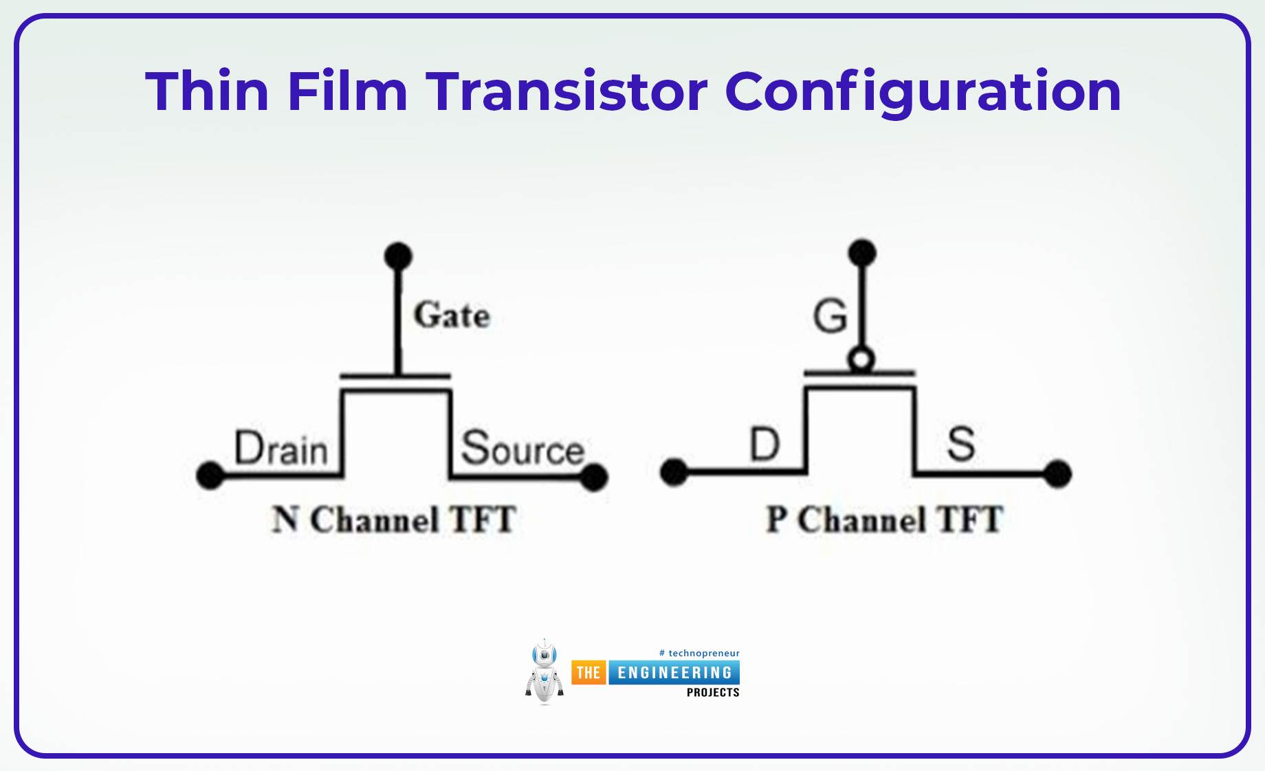
Thin Film Transistor NPN Configuration
The NPN TFT consists of a configuration in which the P-type material is sandwiched between two N-type semiconductor materials. As a result, when the voltage is applied to the gate, the electrons are the main charge carriers, and the current flows from the emitter to the collector.
Thin Film Transistor PNP Configuration
The PNP TFT has the arrangement of the two p-type semiconductor layers on the sides of the N-type material. As a result, on the voltage application on the gate, the hole flows from the emitter to the collector and serves as the main charge carrier.
Thin Film Transistor History
Over the past fifty years, thin film translators have changed, updated, and improved, and the story of its life is quite innovative. Here is an overview of the history of thin film transistors and how they have made their place in modern display electronics.
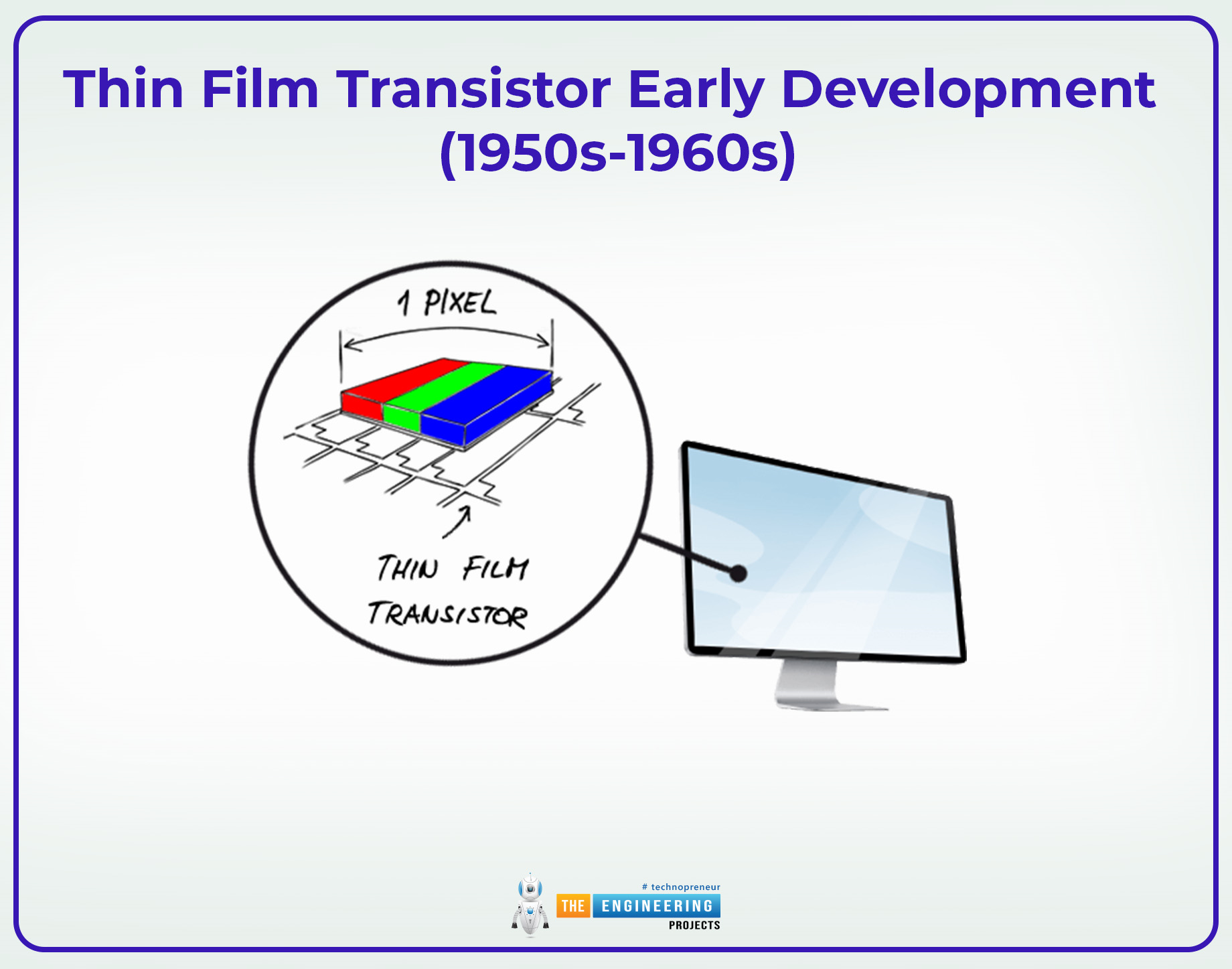
Thin Film Transistor Early Development (1950s-1960s)
In the early 20th century, the physicist Julius Lilienfeld proposed the concept of a field-effect transistor (FET). At that time, this concept did not get that much importance to be utilised int the practical work. However, working on the FETs gained popularity in the 1950s and this has changed the whole era.
In 1947, John Bardeen, Walter Brattain, and William Shockley, working in the Bell lab, invented the bipolar junction transistor (BJT), and this revolutionized the whole electronic world. This breakthrough led to the invention of other types of transistors.
In 1962, the first thin film transistor was developed at the RCA laboratories by Paul K. Weimer. This work acted as a groundbreaking because he has fabricated the transistor on the insulating material that no one did before. Till then, transistors were made only on silicon wafers, but Weimer created the transistor with flexible, transparent, and insulated material, and this acted as the base of transparent and better electronic displays.
Thin Film Tnrasistor Progress Era (1970s-1980s)
In this decade, the thin film transistor gained popularity and this led the researchers to work and experiment on this transistor to make it even better. This is specifically renowned for the introduction and usage of amorphous silicon (a-Si) as the semiconductor material for this transistor.
In 1979, T. Brody developed amorphous silicon-based TFTs and therefore, is often regarded as the "father of the flat-panel display,” because of his work on active-matrix liquid crystal displays (AMLCDs). He knew the properties of the amorphous silicon in TFTs and worked on it in detail. According to him, it can be easily used on large surface areas and has a simple fabrication process even for thin films.
Before the introduction of thin film transistors, televisions, monitors, and other displays used thick and heavy cathode-ray tubes (CRTs). Yet, after the successful work on the thin film transistors, liquid crystal displays (LCDs) gained traction and took the place of CRTs.
Early LCDs used passive-matrix displays that had some disadvantages, such as slow response or low image quality. Applying the TFTs in these displays solved these problems and played a crucial role in the success of LCDs. The latest LCDs use AMLCD technology that provides quick response, high quality, captivating colors, and, as a whole, the best quality displays.
Thin Film Transistor Application Commercialization (1990s-2000s)
In the 1990s, experimentation and research made it possible to represent the TFT displays for commercial use. The introduction of these displays in the market has made the rapid adoption of thin film transistor applications in several devices.
This was the time when the TFT LCDs were dominating other display technologies for commercial purposes. Companies like Sony, Samsung, and others were adopting this for the displays of computers, laptops, televisions, and other small to large-scale displays. The low power usage, high-quality display, and flat surface display were the major qualities that dominated the large and heavy CRT-based TVs.
In 1998, the electronics company “Sharp" commercially displayed the first TFT-LCD TV, which was a major milestone for the conversion of CRT-based displays to TFT LCDs. This has made major changes in the whole electronics companies' milestones and working methods.
Thin Film Transistor Displays Advancements (2000s-2010s)
The new century is considered the advancement era with respect to the thin film translator displays. Not only the displays but also the transistors themselves bear many updating processes and this has made the transistor even better.
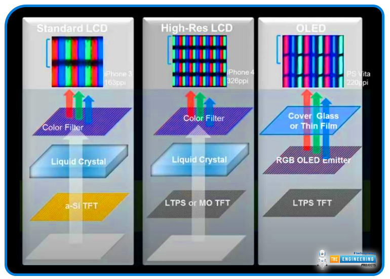
Till the 1990s, amorphous silicon transistors were in use but in the 2000s, polysilicon (p-Si) was introduced as the material for thin film transistors and this has made many changes in its output. Polysilicon has higher mobility than amorphous silicon; therefore, it shows a faster-switching property and, as a result, provides better display quality. The high resolution has made it eligible for better smartphones, digital cameras, and OLED displays.
It seems like the working and experimentation on the thin film transistors never stopped because, in 2012, Indium Gallium Zinc Oxide (IGZO) was introduced as the base material for their production. It offers even faster mobility and low power consumption and thus was considered the best choice for the 4K and 8K displays. The estimate of this technology can be done by knowing the fact that IGZO technology was used by the Apple company for the iPad Pro and MacBook line displays.
After this, the market wanted to do something new and better so they started working on the foldable displays. This demand of foldable and flexible devices has intensified the researchers to work on the foldable transistors. As a result, the organic TFTs (OTFTs) came into the conversion that made the displays foldable, rollable, bendable, and provided the best performance. This has revolutionized the electronic industry and the work on wearables and other such displays and devices was the main focus of the companies.
Currently, the work on the thin film transits is still at its peak, and experts are working on making it better with respect to performance, reliability, and quality. You will learn about the latest trends and work at the end of this article, where we’ll be discussing the TFT applications.
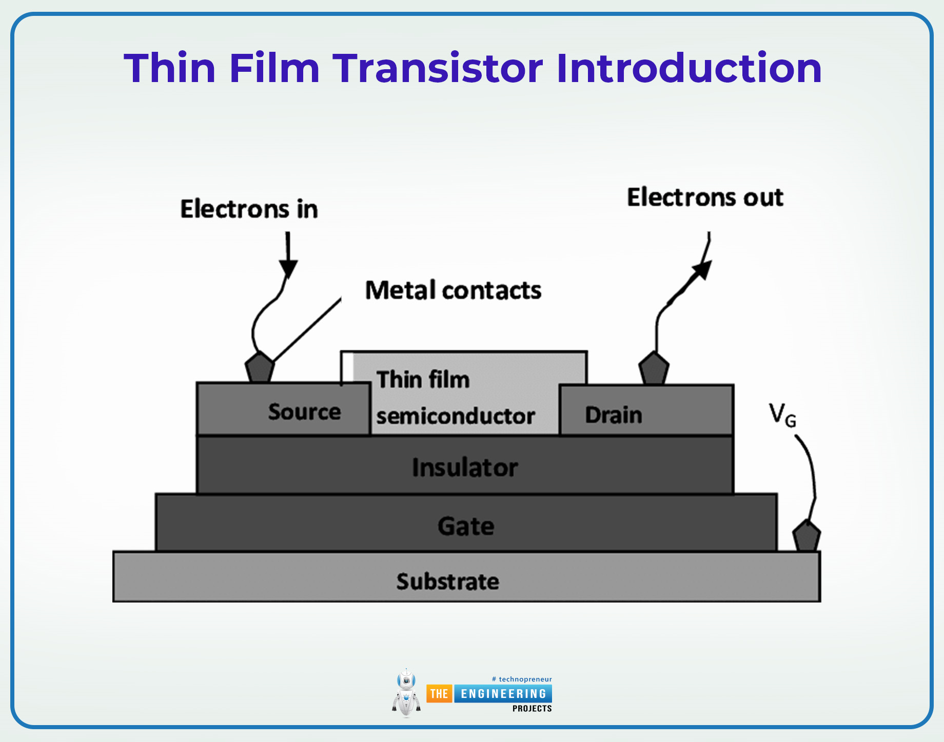
Thin Film Transistor Structure
The structure of the thin film transistor resembles the other types of field effect transistors. The transistor has three terminals and the introduction of each of them is given in the table below:
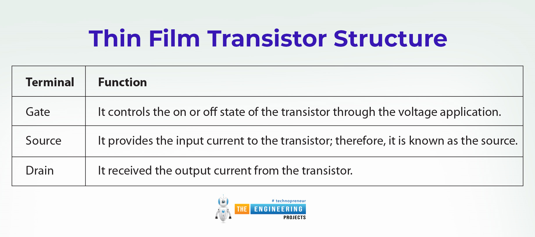
Terminal |
Function |
Gate |
It controls the on or off state of the transistor through the voltage application. |
Source |
It provides the input current to the transistor; therefore, it is known as the source. |
Drain |
It received the output current from the transistor. |
Thin Film Transistor Key Components
Let’s define the thin film transistor again with respect to its structure:
“It is a specialized form of field-effect transistor (FET) in which a thin layer of the active semiconductor layer with dialect layers and metallic contacts is deposited on the supporting substrate.”
The following are the basic key components of the thin film transistors:
Thin Film Transistor Substrate
This is the base material at which the thin film transistor layer is deposited. It provides the foundation of the transistor and is crucial for supporting the whole TFT structure. The older versions of TFT were made of glass and the newer ones use flexible plastic as substrate. The TFTs made with the glass substrates are used in the TFT LCDs and plastic and polymer transistors are usually designed for flexible displays, foldable devices, etc.
Thin Film Transistor Semiconductor Layer
The purpose of a semiconductor layer is to act as the channel between the source and drain terminals for the electron flow when the gate terminal is applied. We have discussed all these in the history section of this article. The following is the detail of the semiconductor layer material along with their specifications:
Amorphous silicon is a low-cost semiconductor material that is widely used in traditional LCDs.
Polysilicon (p-Si) has higher electron mobility than amorphous silicon and provides a fast switching speed; therefore, it is considered a good choice for high-resolution and demanding electronic displays.
The Indium Gallium Zinc Oxide (IGZO) also has fast electron mobility and provides transparency; therefore, it is usually utilized in advanced resolution displays that require low power consumption.
Organic semiconductors are used in the latest and most advanced technologies and where the companies require flexible displays.
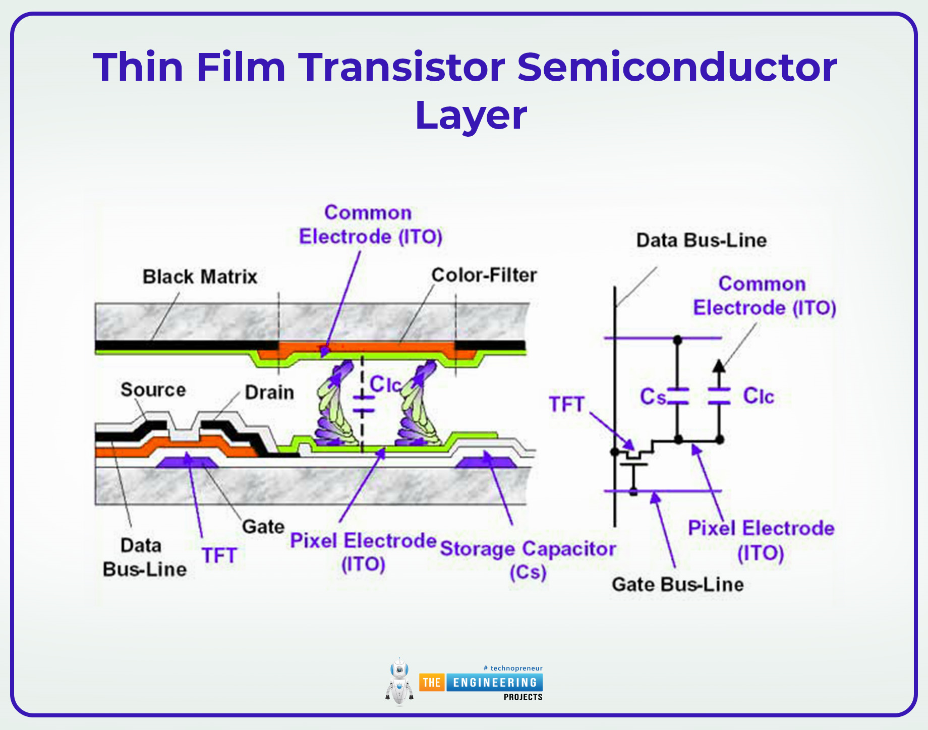
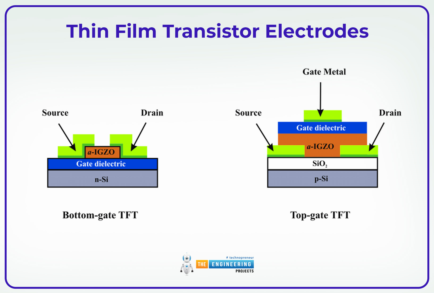
Thin Film Transistor Gate Electrodes
The gate electrodes are the conductive material that controls the current flow through the source to the drain. It applied the voltage that influences the semiconductor layer beneath the gate. It is typically made of aluminum (Al), molybdenum (Mo), chromium (Cr), and other metals. The gate electrode is situated on one side of the thin dialect layer and forms the parallel capacitor with the channel.
Thin Film Transistor Gate Dielect
It is the thin layer of insulating material that electrically isolates the gate electrode from the semiconductor material. It is so thin as to allow the electrical field to influence the semiconductor's conductivity. The common materials used in the gate dialect are silicon dioxide (SiO₂) or silicon nitride (Si₃N₄).
The thickness of this layer is crucial to the thin film transistor's performance because it determines the efficiency of the gate to control the transistor.
Thin Film Transistor Electrodes
The source and drain electrodes are made with highly efficient conducting materials such as aluminum (Al), gold (Au), or silver (Ag). The source provides the electrons or hole supply (depending on the type of semiconductor material), whereas the drain collects the electrons once they have been traveled through the semiconductor material.
The source and drain electrodes work with the gate and provide the current flow through the transistor in order to provide the main working of the transistor.
Thin Film Transistor Channel
The channel is the transistor’s area of the semiconductor layer where the charges move (either hole or electron) when the voltage is applied to the gate terminal, that is when the transistor is turned on. This voltage results in the charge induction in the semiconductor material and this creates the conductive path between the source and the drain.
Thin Film Transistor Passivation Layer
The passivation layer is responsible for the protection of the transistor from moisture, dust, and other contaminants to maintain its performance. It is usually made of a dielectric material like silicon nitride (Si₃N₄). This layer is responsible for the transistor’s long life and reliability.
Thin Film Transistor Working
The thin film transistor is a type of field effect transistor (FET) that follows the principle of modulating electrical conductivity and works through the electrical field. These are the tiny switches that change their on/off situation quickly and charge the pixel accordingly. The state of the thin film transistor or, in return, the pixel’s properties result in the formation of the display. Hundreds of thousands of pixels collectively create the images on the devices, and the combination of brightness, on, off, and other features collectively creates the videos on the devices. The details of the thin film transistor’s working are described below:
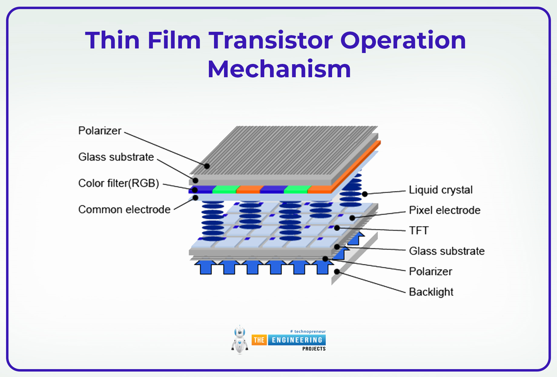
Thin Film Transistor Operation Mechanism
There are two operating states for the thin film transistor:
When no voltage is applied to the gate terminal of a thin film transistor, it is considered off. At this point, there is no conductive path between the source and drain; therefore, no current flows through the transistor. In the display applications, the pixel does not have any output.
When the positive voltage is applied to the gate terminal, it creates a conductive path from source to drain and the current can now pass through the transistor. As a result, the pixel of the display device is then charged or discharged according to the current flow. This either turns the pixel on or changes its brightness and the combination of these pixels makes the picture on the display devices.
The state of the transistor is decided on the basis of threshold voltage (Vth), which is defined as:
“The threshold voltage (Vth) of the thin film transistor is the minimum voltage that is required to turn the transistor on.”
Below this voltage, the transistor is off, and vice versa. The typical threshold voltage depends on the transistor's internal structure and specifications. Usually, lower threshold values are preferable for better performance at low voltage.
Thin Film Transistor Pexel Charging
In the display devices, the TFT acts as a switch to change the pixel state. In the on state, the TFT allows the current flow towards the pixel and charges it until the next cycle. The voltage applied to the transistor decides the amount of current passing to the pixel and that is responsible for the pixel brightness.
A capacitor is usually added to each pixel to retain the transistor’s charges until the next refresh cycle. The rapid on/off situation of the transistor results in the brightness, illumination, and off state of the pixel. A reason to consider the TFTs best for the display is the analog control of the transistor’s state. The amount of current passing through the source to the drain can be controlled in an analog manner; therefore, the pixel brightness and picture quality may vary.
Thin Film Transistor Types
The table below shows the fundamental types of thin film transistors along with the material used in the manufacturing as well as the basic features:
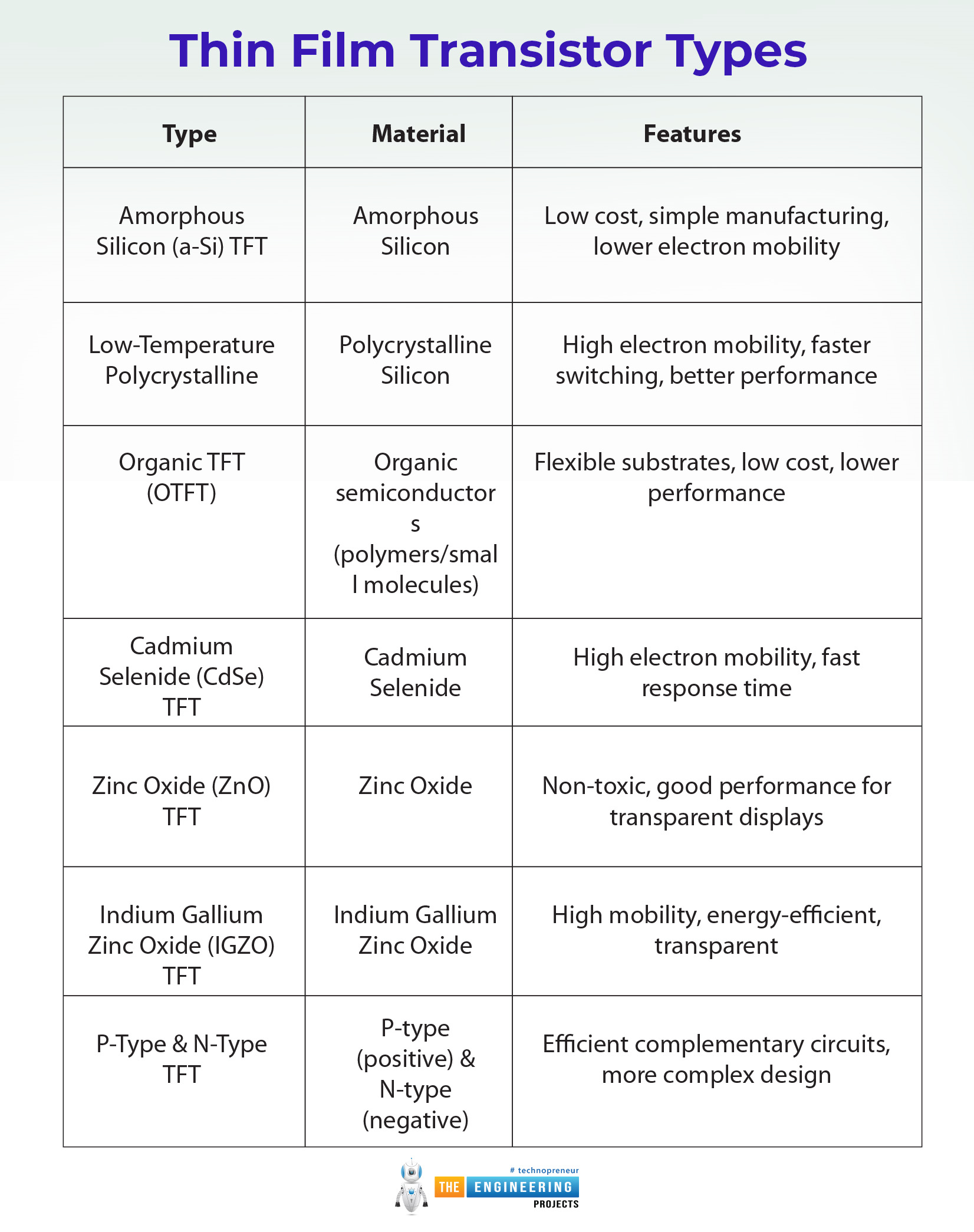
Type |
Material |
Features |
Amorphous Silicon (a-Si) TFT |
Amorphous Silicon |
Low cost, simple manufacturing, lower electron mobility |
Low-Temperature Polycrystalline |
Polycrystalline Silicon |
High electron mobility, faster switching, better performance |
Organic TFT (OTFT) |
Organic semiconductors (polymers/small molecules) |
Flexible substrates, low cost, lower performance |
Cadmium Selenide (CdSe) TFT |
Cadmium Selenide |
High electron mobility, fast response time |
Zinc Oxide (ZnO) TFT |
Zinc Oxide |
Non-toxic, good performance for transparent displays |
Indium Gallium Zinc Oxide (IGZO) TFT |
Indium Gallium Zinc Oxide |
High mobility, energy-efficient, transparent |
P-Type & N-Type TFT |
P-type (positive) & N-type (negative) |
Efficient complementary circuits, more complex design |
Thin Film Transistor Fabrication Process
The fabrication process of thin film transistors involves several steps in a clean and contamination-free environment. The process varies for TFT types but here is a general outline of the processes required for thin film transistor fabrication:
Thin Film Transistor Substrate Preparation
The first step in the fabrication process is the preparation of the substrate material. As mentioned before, traditional TFTs use rigid material, such as glass, as the substrate, whereas, the latest TFTs have flexible material, such as transparent, as the substrate.
The preparation process just involves thoroughly cleaning of the substrate surface to remove any particles or impurities. This seems a simple process but it ensures that the TFT’s performance is not affected by unwanted particles. Based on the type of substrate, the chemical or base is applied to the surface.
Thin Film Transistor Gate Material Deposition
The step involves the gate electrode deposition on the substrate. The gates are made with reactive materials like aluminum, gold, or chromium, and different techniques are applied for the deposition. The two most common are:
Physical vapor deposition (PVD)
Chemical vapor deposition (CVD)
Usually, photolithography is the technique applied for the pattern formation of the gate electrode. It involves the application of photoresist material on the surface. After that, the material is then exposed to the light for the right pattern formation.
Thin Film Transistor Gate Insulation
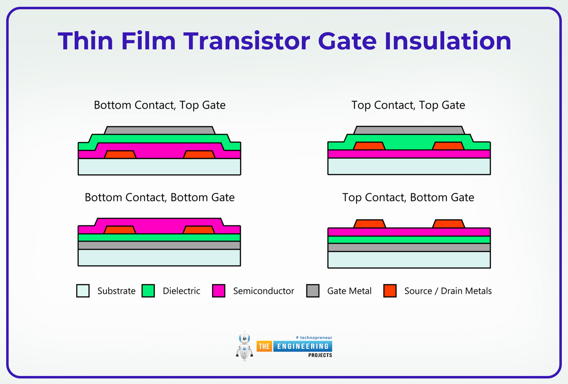
The gate insulator layer electrically insulates and separates the gate from the source and drain terminals. Hence, a thin film is applied to the gate that is typically made of silicon dioxide (SiO₂) or silicon nitride (Si₃N₄). Plasma-enhanced chemical vapor deposition (PECVD) and sputtering are the common techniques for such processes.
Thin Film Transistor Semiconductor Layer Deposition
Based on the type of the thin film transistor, the semiconductor layer is applied to the product formed till now. The common materials for this layer are amorphous silicon (a-Si), polycrystalline silicon (p-Si), or organic material for organic TFTs (OTFT), and the processes involved are PECVD, CVD, or spin-coating (for organic materials).
Thin Film Transistors Source and Drain Formation
Just like the pattern process of a gate electrode, the source and drain use photolithography technology for the source and drain formation. Once this process is complete after the light exposition, the excess metal is removed from the surface using the wet etching or dry etching process to get clean and precise patterns.
This step involves the use of PVD or CVD techniques for the source or drain terminal formation that is also made of aluminum, gold, or chromium. After this step, our three terminals of the TFT are now formed successfully.
Thin Film Transistor Testing and Quality Control
This is the final step that ensures the perfect quality and performance of the TFT. After the fabrication process, the TFT is now ready for the work, but the electrical testing is done on the transistors to see if they are working ideally. The whole yield is monitored under strict parameters and the only transistors passing this test are sent to the market.
Note: for some types of TFTs, the channel formed during the fabrication process is doped to get the required electrical properties. Moreover, processes like passivation layer formation and annealing are optional during manufacturing and depend on the fabrication team’s choice.
Thin Film Transistor Key Characteristics
Here are the basic characteristics of the thin film transistors that make them different from the other types of transistors:
Thin Film Structure
The TFTs, as expected from the name, contain a very thin layer of conductors, semiconductors, or insulators on the substrate. The thickness of this film ranges from nanometers to a few micrometers.
Thin Film Transistor Low Power Consumption
The low power consumption feature of this transistor makes it an ideal choice for the devices working on the battery or require low power feature. It consumes very low energy, especially for static images.
Thin Film Transistor High Switching Speed
The TFTs have a higher switching speed than other types. The rapid rate of high/low states makes it ideal for high-speed applications like display devices that require a quick pixel refresh. Polycrystalline silicon (p-Si) TFTs have an even more rapid rate of switching as compared to the amorphous silicon TFTs.
Thin Film Transistors Pixel Control
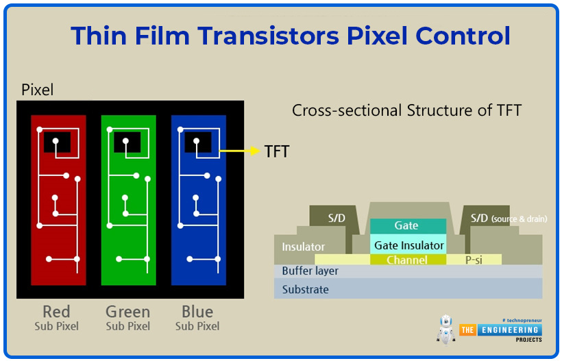
The thin film transistors have precise pixel control and the analog current control makes it a good choice for the varying brightness of the pixels. The TFTs allow the individual control of each pixel, which results in a sharp display and better color contrast as compared to other transistor types.
Thin Film Transistor Flexible Substrate
This is a unique feature that justifies the popularity of this transistor. The flexible substrate helps the transistor to be used in wearables, flexible displays, mobiles, and other such devices. Organic TFTs (OTFTs) are the ideal choice for flexible electronics because they work in low-temperature ranges and have a high flexibility rate.
Thin Film Transistor High Mobility
When dealing with display devices, the mobility rate is a crucial parameter. It is defined as:
“The carrier mobility is the rate at which the charge carriers (hole or electrons) can move through the semiconductor material.”
The higher mobility rate means fast switching and the TFTs have a great mobility rate. The p-Si TFTs have an even higher mobility rate as compared to the a-Si TFTs; therefore, they are a preferable choice for high-resolution and high-speed applications such as smartphones.
Thin Film Transistor Transparency
The thin film transistor is made with transparent material as the substrate, conductive layer, and semiconductor layer. Hence, these provide a transparent appearance and are the perfect choice for applications like augmented reality displays, head-up displays, etc.
Thin Film Transistor Cost
The thin film transistor is considered the cost-effective choice because the fabrication process of these transistors is uncomplicated and does not require a high cost and heavy equipment. Moreover, in large-scale production, the cost is reduced more, and cost is the basic consideration when choosing any electronic device.
Thin Film Transistor VS Traditional Transistors
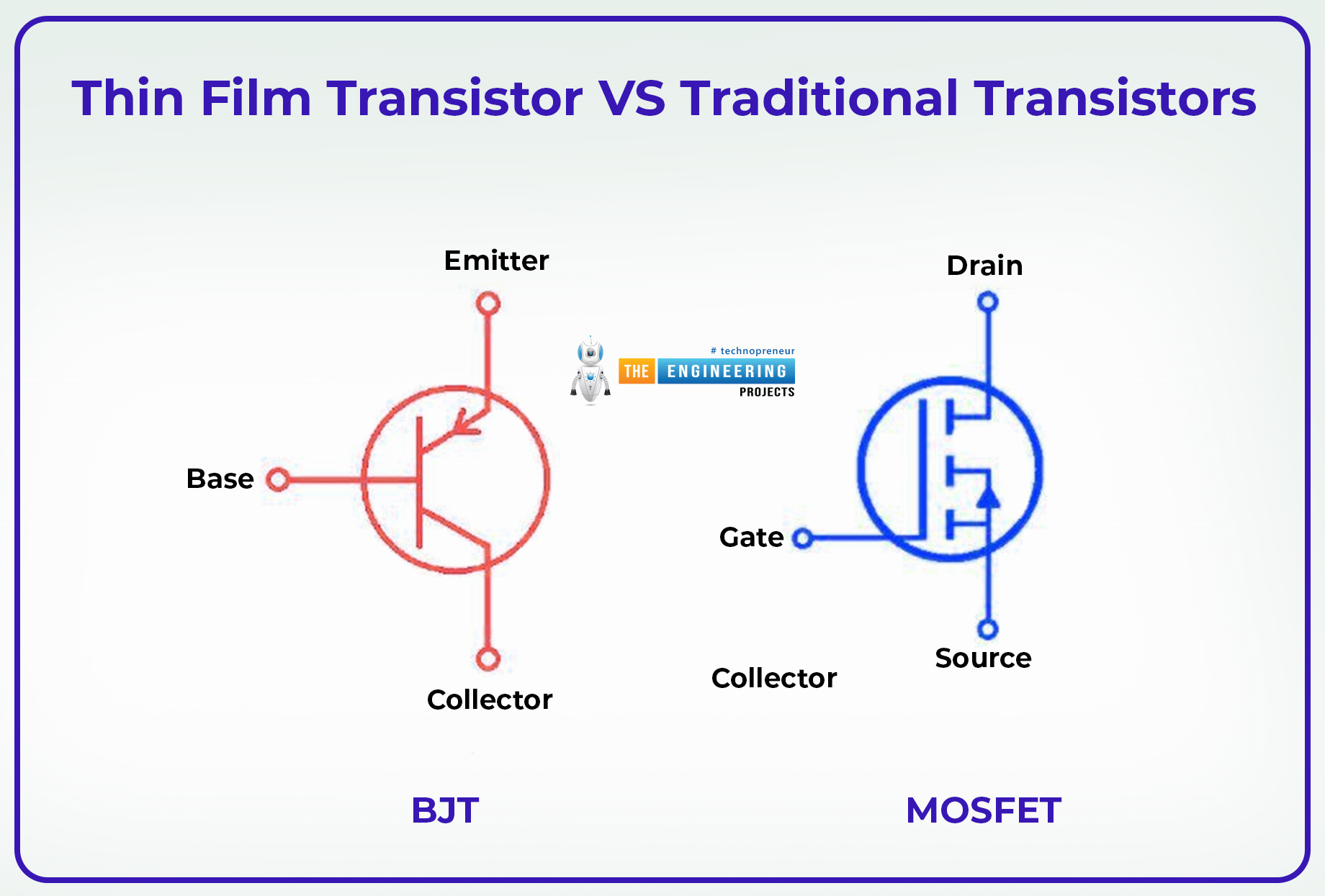
The thin film translator is a type of Metal-Oxide-Semiconductor Field-Effect Transistor (MOSFET) but it has several distinctions from the traditional transistors. The following is the comparison between the TFTs, MOSFETs, and bipolar junction transistors (BJT) that will help you to understand the reason behind the TFT's popularity for display devices.
Fabrication Process
The main distinction between the transistors is the fabrication process that decides its features and applications. The TFTs are made by depositing a thin film of semiconductor material on the glass or plastic substrate.
On the other hand, the traditional transistors are made through the fabrication process on silicon wafers, which are bulky and cost more. This is the reason why these transistors require complex and rigid substrates. This not only limits the applications of traditional transistors to power electronics and integrated circuits but also requires a more technical fabrication process.
Application Domain
Thin film transistors have applications mainly in display devices such as liquid crystal displays (LCDs), monitors, mobile displays, etc. where there is a need to control each pixel through the transistor and the particular analog current is required. It is an ideal choice for large surface area applications and electronics requiring a flexible and transparent substrate.
On the contrary, the BJTs are usually considered a good choice for the switching devices and amplification process. This is used in the audio devices that require the frequency change, such as the radio and other devices.
The MOSFET has applications in digital electronics, power control microprocessors, digital devices, and many others. The power electronics have several applications of MOSFET.
Operating Principle
The thin film transistor is the type of field effect transistor so the gate terminal controls the current flowing through the source to the drain through the semiconductor channel. The operating principle of MSOFET is the same as the TFT, where the voltage controls the working of the transistor but the bipolar junction transistor has a different operating mechanism than these two. It is controlled by the current flow through the base terminal; hence, the base controls the source and drain.
Size and Power Consumption
The thin film transistor is different from other transistor family members with respect to size, performance, and power consumption. The core reasons are its fabrication process and internal structure. These are very thin and are designed for transparent screens or other display screens. These are lightweight transistors and require less space; therefore, they are suitable for applications requiring such features.
On the other side, the BJT and MOSFET are bulky and require more space than the thin film transistors. These are not suitable for display devices but are part of large circuits such as microcontrollers.
The table below has the summary of all the discussion about the difference between these three basic types of transistors that will help you to understand the topic in just a glance:
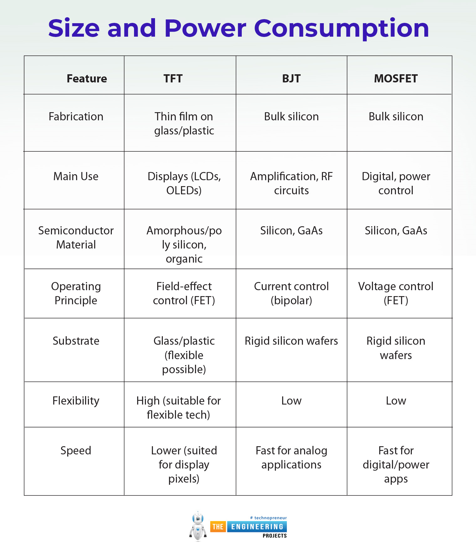
Feature |
TFT |
BJT |
MOSFET |
Fabrication |
Thin film on glass/plastic |
Bulk silicon |
Bulk silicon |
Main Use |
Displays (LCDs, OLEDs) |
Amplification, RF circuits |
Digital, power control |
Semiconductor Material |
Amorphous/poly silicon, organic |
Silicon, GaAs |
Silicon, GaAs |
Operating Principle |
Field-effect control (FET) |
Current control (bipolar) |
Voltage control (FET) |
Substrate |
Glass/plastic (flexible possible) |
Rigid silicon wafers |
Rigid silicon wafers |
Flexibility |
High (suitable for flexible tech) |
Low |
Low |
Speed |
Lower (suited for display pixels) |
Fast for analog applications |
Fast for digital/power apps |
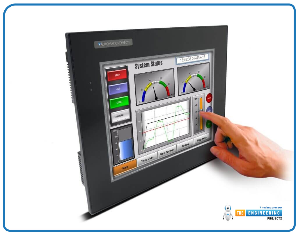
Thin Film Transistor Use in Displays
As discussed before, thin film transistors have a significant role in revolutionizing the display device industry. The impact is so strong that TFTs are the ideal choice for almost every type of display screen. Here are some fundamental real-life applications that have been made extraordinary because of the thin film transistor involvement.
Thin Film Transistors in LCDs
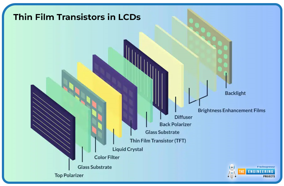
The thin film transistors are the main technology behind liquid crystal displays (LCDs). The active matrix controls the brightness, states, and working of each individual pixel for the sharp and smooth transitions in the videos. This feature has created room for other display technologies using the same technique. As a result, the thin film transistors are the backbone of several display devices ranging from small smartphones to large surface LCD monitors and televisions.
Thin Film Transistor in Electronic Paper Display
The electronic paper display (EPD) devices are designed for the paper-like reading experience with low power consumption and less retention for the eyes. These devices use thin film transistors for high contrast and pixel control with high resolution.
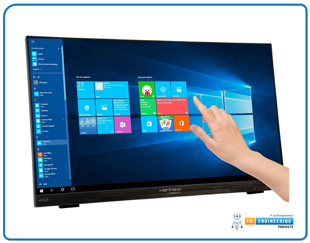
Thin Film Transistor in Touch Screens
A great variety of display devices enable touch screen control and such displays are made with thin film transistors that provide a smooth experience and accuracy in touch screens and result in a more user-friendly interface.
Thin Film Transistors in Medical Imaging
Medical imaging devices are now becoming more attractive and intuitive and thin film transistors have a role in it. These transistors provide high-resolution X-rays, CT scans, and other devices with great details on the results. Moreover, the low power-consuming displays make it easy for the manufacturers to create battery-oriented devices that can be remotely used.
Thin Film Transistor in Automotive Displays
The automotive displays require a technique with low power consumption and flexibility, so thin film transistors are the ideal choice. These are used in the car dashboard, infotainment displays, and even the traffic signs in some areas. This provides the drivers with a good environment with respect to entertainment, information, and clear visibility at low power consumption.
Thin Film Transistor in Industrial Automation
The industries are moving towards automation and intelligent systems and this requires monitoring and visual inquiry for critical monitoring. This has enhanced the need and use of thin film transistor displays in industries because these are lightweight screens and can be utilized at any place for continuous use.
Thin Film Transistor for Scientific Instruments
The latest scientific instruments show automatic calculation and measurement and for this, they require a high-definition display that shows the small digits and reading without any visual error. The thin film transistors are present in the modern oscilloscope, electron microscope, and other such instruments.
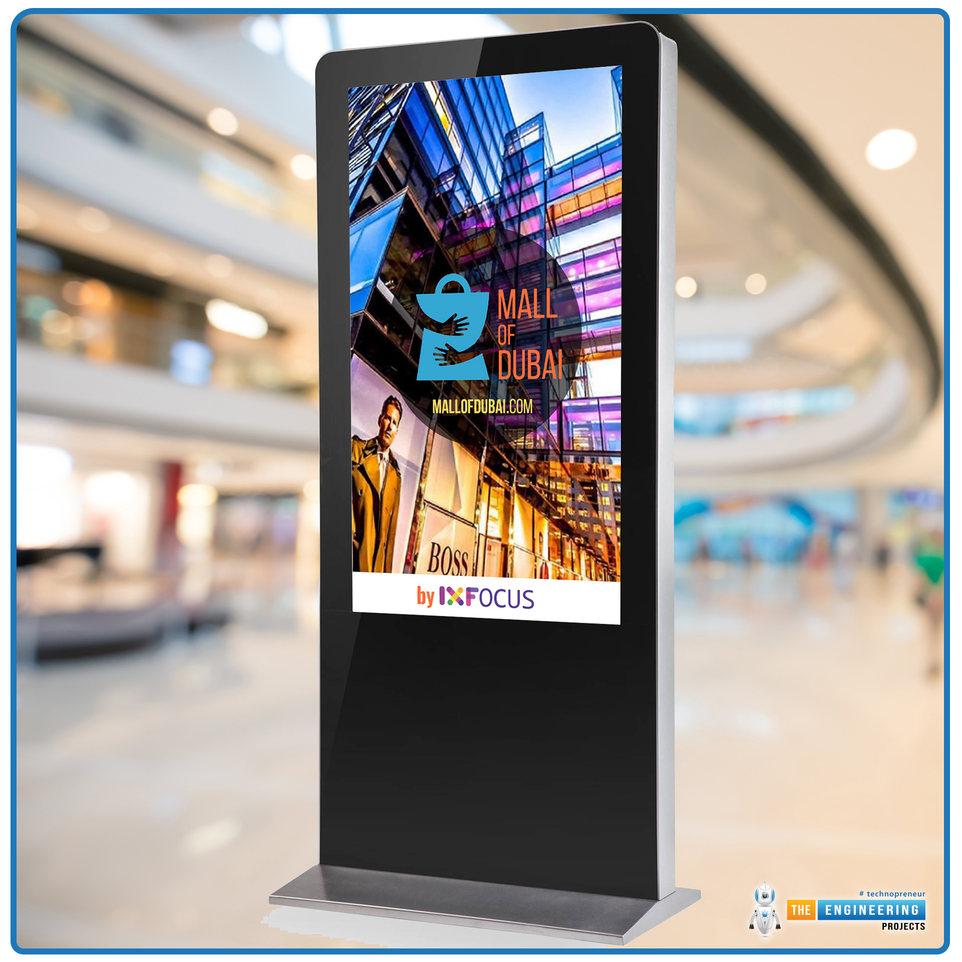
Thin Film Transistors in Digital Signage
A significant example of the applications using thin film transistors is digital signage, which makes electronic advertisement inexpensive, durable, and prominent. Digital billboards, public display messages, advertisement screens, and gigantic-sized liquid display screens use thin film transistors for the illumination of a large number of pixels at high resolution.
Thin Film Transistor Disadvantages
Thin film transistors are the popular choice for modern electronic displays but they have some limitations as compared to some other options and the discussion can not be completed until we mention them:
Thin Film Transistor Limited Viewing Angle
The biggest disadvantage that is the reason to move towards the other latest technologies is the limited view angle of TFT. We all have experienced the issue of LCDs where the side angle of the display may show the screen with the least brightness or distortion. The TFT only shows the right pixel brightness from the front and for the big screens where more than one viewer is using the display may show the incomplete view.
Thin Film Transistor Low Response Rate
The TFT has a low response time as compared to some other latest techniques, such as OLED, and plasma. In some applications, the TFT shows the motion blue and this is especially true for high-speed display applications such as high-definition video games.
Thin Film Transistor Uniformity Issues
In the case of some TFT applications, the back bleeding and inconsistent image quality fail the thin film transistor in some severe weather, load, or speed applications.
Thin film transistors are one of the most dominant devices for display devices because of their reliability, performance, low power consumption, inexpensive fabrication, and other features. The foldable screens and the high-resolution displays are usually made of thin film transistors. There are some limitations of TFT when compared with the most updated techniques of this era but overall, we can say that TFT has revolutionized the display screen industries.