MJE13007 NPN Transistor Datasheet, Pinout, Features & Applications


Hello Everyone! Happy to see you around. Thank you for clicking this read. In this post today, I’ll document the Introduction to MJE13007. MJE13007 is an NPN bipolar junction transistor that is a semiconductor device made of silicon material. This chip is mainly used for amplification and switching purposes. The collector-base voltage is 700V while the collector-emitter voltage is 400V. The power dissipation at temp 25C is 80W. This means 80W is released during the working of this device. This device can support load up to 8A because the current at the collector side is 8A. I suggest you read this entire post till the end as I’ll include the complete Introduction to MJE13007 covering datasheet, pinout, working principle, power ratings, applications, and physical dimensions. Let’s get started.
Introduction to MJE13007
- MJE13007 is an NPN bipolar junction transistor mainly used for high voltage high-speed switching applications.
- Three layers are used for the construction of this device. One is a p-doped layer that stands between two n-doped layers.
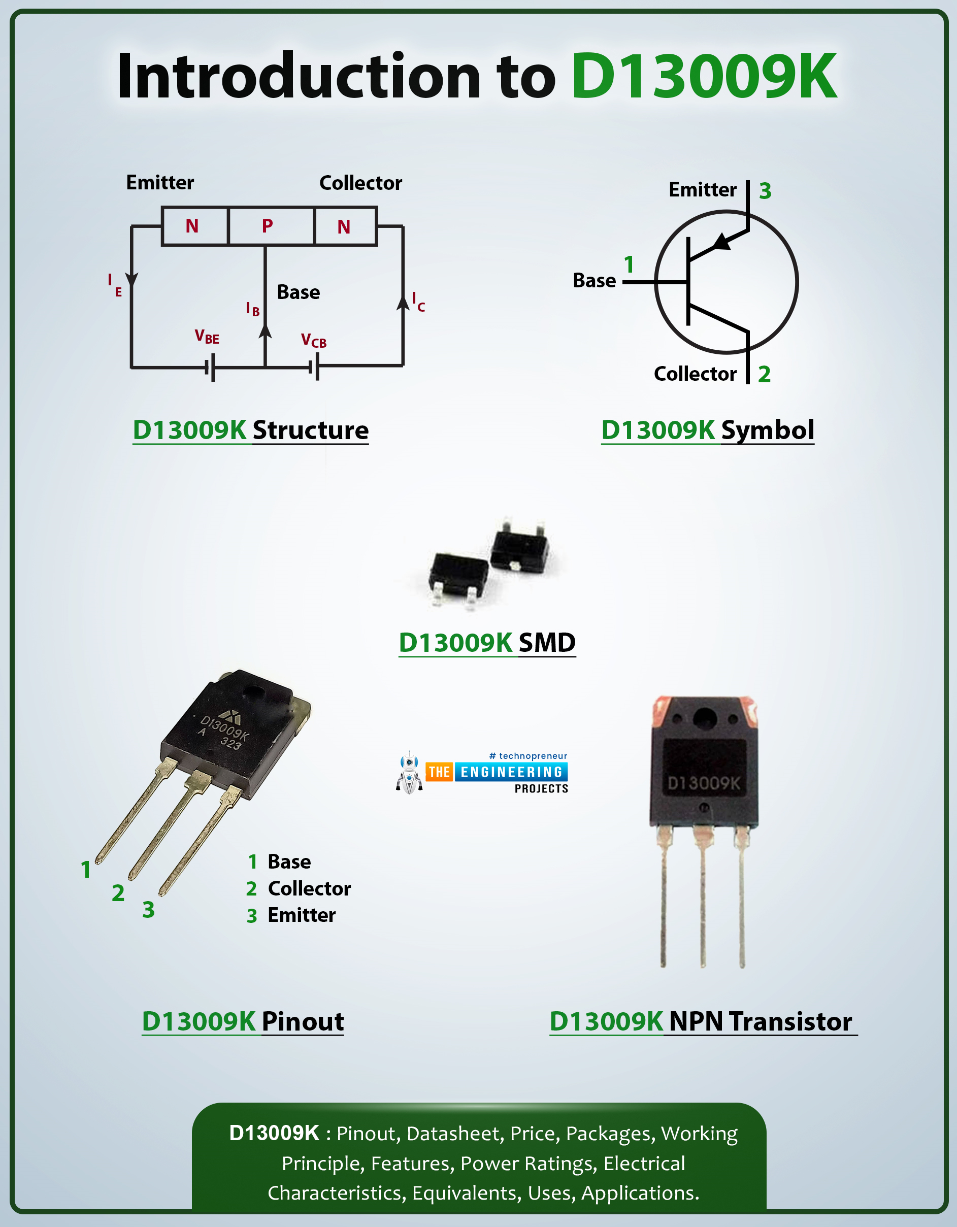
- MJE13007 includes three terminals named base, collector, and emitter. The small input current at the base side is used to generate a large output current across the emitter and collector terminals.

- The emitter-base voltage is 9V which means this device requires 9V to initiate the transistor action.
- Bipolar junction transistors come in two types i.e. NPN transistors and PNP transistors. This device MJE13007 falls under the category of NPN transistors where electrons are the major carriers while in the case of PNP transistors holes are the major carriers.
- It is important to note that in bipolar junction transistors both electrons and holes are involved in the conductivity inside the transistors but holes are majority carriers in PNP transistors while electrons are major carriers in NPN transistors.
- The mobility of holes is less efficient than the mobility of electrons, making NPN transistors a better choice for the range of applications.
- Moreover, the current flows from emitter to collector in PNP transistors while it flows from collector to emitter in NPN transistors.
- Transistors are mainly divided into two main types’ i.e. bipolar junction transistors and MOSFETs. The bipolar junction transistor are the current-controlled device while MOSFETs are the voltage-controlled devices that include terminals known as a drain, source, and gate.
MJE13007 Datasheet
Before you apply this device to your electrical project, it is wise to scan through the datasheet of the device that details the main characteristics of the device. Click the link below to download the datasheet of MJE13007.MJE13007 Pinout
The MJE13007 includes three terminals named:- Base
- Collector
- Emitter


MJE13007 Working Principle
- The base side is responsible for the overall transistor action. When voltage is applied at the base pin, it gets biased, and current will start flowing from the collector to the emitter terminal.
- This device MJE13007 is not a symmetrical device. The lack of symmetry is due to the difference in the doping concentration of all three terminals.

- If you try to exchange the emitter and collector terminals, it will prevent the device from working in forward active mode and as a result, both terminals will start working in reverse active mode, influencing the values of both common-emitter current gain and common-base current gain.
| Absolute Maximum Ratings of MJE13007 | ||||
|---|---|---|---|---|
| Pin No. | Pin Description | Pin Name | ||
| 1 | Collector-emitter voltage | 400V | ||
| 2 | Collector-base voltage | 700V | ||
| 3 | Base-emitter voltage | 9V | ||
| 4 | Collector current | 8A | ||
| 5 | Power dissipation | 80W | ||
| 6 | Base current | 4A | ||
| 7 | Operating and storage junction temperature range | -55 to 150C | ||
- The power dissipation is 80W which is the amount of power that will dissipate during the working of this device. The collector-base voltage is 700V and the collector-emitter voltage is 400V.
- The emitter-base voltage is 9V which is the amount of voltage that you will apply to bias the device and start the transistor action.
- When you’re working with this chip, make sure the ratings don’t exceed the absolute maximum ratings. Otherwise, they can severely damage the device, thus the entire project.
- Moreover, don’t apply these ratings more than the desired time, else they can affect device reliability.
MJE13007 Applications
The following are the main applications of the MJE13007 NPN transistor.- Incorporated in modern electronic circuits.
- Employed in the switched-mode power supply.
- Employed to support loads under 8A.
- Installed in the motor control circuit.
- Used in voltage regulator circuits.
- Used for switching and amplification purpose.
- Used in H-bridge circuits.
- Used in Bistable and Astable multivibrators circuit.
MJE13007 Physical Dimensions
The following figure presents the physical dimensions of MJE13007.