


74LS138 - 3 to 8 Line Decoder IC | Datasheet, Working and Simulation


Hello students! I hope you are doing great. Today, we are talking about the decoders in the proteus. We know that decoders are the building blocks of any digital electronic device. These electronic circuits are used for different purposes, such as memory addressing, signal demultiplexing, and control signal generation. These decoders have different types and we are discussing the 3 to 8 line decoders.
In this tutorial, we will start learning the basic concept of decoders. We’ll also understand what the 3-to-8line decoders are and how we connect this concept with the 74LS138 IC in proteus. We’ll discuss this IC in detail and use it in the project to present the detailed work.
What is a 3 to 8 Line Decoder?
A three to eight line decoder is an electronic device that takes three inputs and based on their combination, provides one of its eight outputs. In simple words, the 3 to 8 line decoder gets three inputs and reads the binary combination of its input. As a result, the single output is obtained at the output of the decoder. Here are the basic concepts to understand its working:
Binary Input in 3 to 8 Decoder
A 3 to 8 line decoder has three input pins which are usually denoted as A, B and C. These correspond to the three bits of the binary code. The term binary means these can only be 0 or 1 and no other digits are allowed. This can be the raw bits from the user or can be the output signal from the circuits’ device that becomes the input of the decoder.
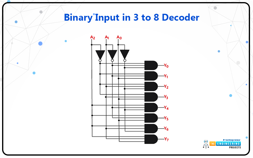
Outputs of 3 to 8 Decoder
The 3 to 8 decoder has eight possible output pins. These are usually denoted as Y0, Y1, Y2,..., Y7 and the output is obtained only at one of these pins. The output depends on the binary combination of the input provided to it. In large circuits, its output is fed into any other component and the circuit works.
Functionality of 3 to 8 Decoder
As mentioned before, the combination of the binary input decides the output. Only one of the eight output pins of the decoder gets high which means, only one output has the value of one and all others are zero. The high pin is considered active and all other pins are said to be inactive.
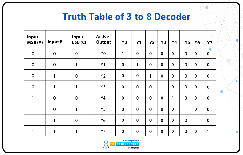
Truth Table of 3 to 8 Decoder
The truth talbe of all the inputs and possible output of 3 to 8 decoders are given here:
Input MSB (A) |
Input B |
Input LSB (C) |
Active Output |
Y0 |
Y1 |
Y2 |
Y3 |
Y4 |
Y5 |
Y6 |
Y7 |
0 |
0 |
0 |
Y0 |
1 |
0 |
0 |
0 |
0 |
0 |
0 |
0 |
0 |
0 |
1 |
Y1 |
0 |
1 |
0 |
0 |
0 |
0 |
0 |
0 |
0 |
1 |
0 |
Y2 |
0 |
0 |
1 |
0 |
0 |
0 |
0 |
0 |
0 |
1 |
1 |
Y3 |
0 |
0 |
0 |
1 |
0 |
0 |
0 |
0 |
1 |
0 |
0 |
Y4 |
0 |
0 |
0 |
0 |
1 |
0 |
0 |
0 |
1 |
0 |
1 |
Y5 |
0 |
0 |
0 |
0 |
0 |
1 |
0 |
0 |
1 |
1 |
0 |
Y6 |
0 |
0 |
0 |
0 |
0 |
0 |
1 |
0 |
1 |
1 |
1 |
Y7 |
0 |
0 |
0 |
0 |
0 |
0 |
0 |
1 |
Here,
MSB= Most significant bit
LSB= Least significant bit
I hope the above concepts are now clear with the help of this truth table.
Introduction to 74LS138 Decoder
The 74LS138 is a popular integrated circuit IC that is commonly used 3 to 8 line decoder. It is one of the members of 74LS therefore, it is named so. The 74LS is a group of transistor transistor logic (TTL) chips. The basic feature of this IC is to get three inputs and provide the signal on only one pin of the output automatically based on the binary inputs. In addition to the input, output, and functionality of the 74LS138, there are some additional features listed below:
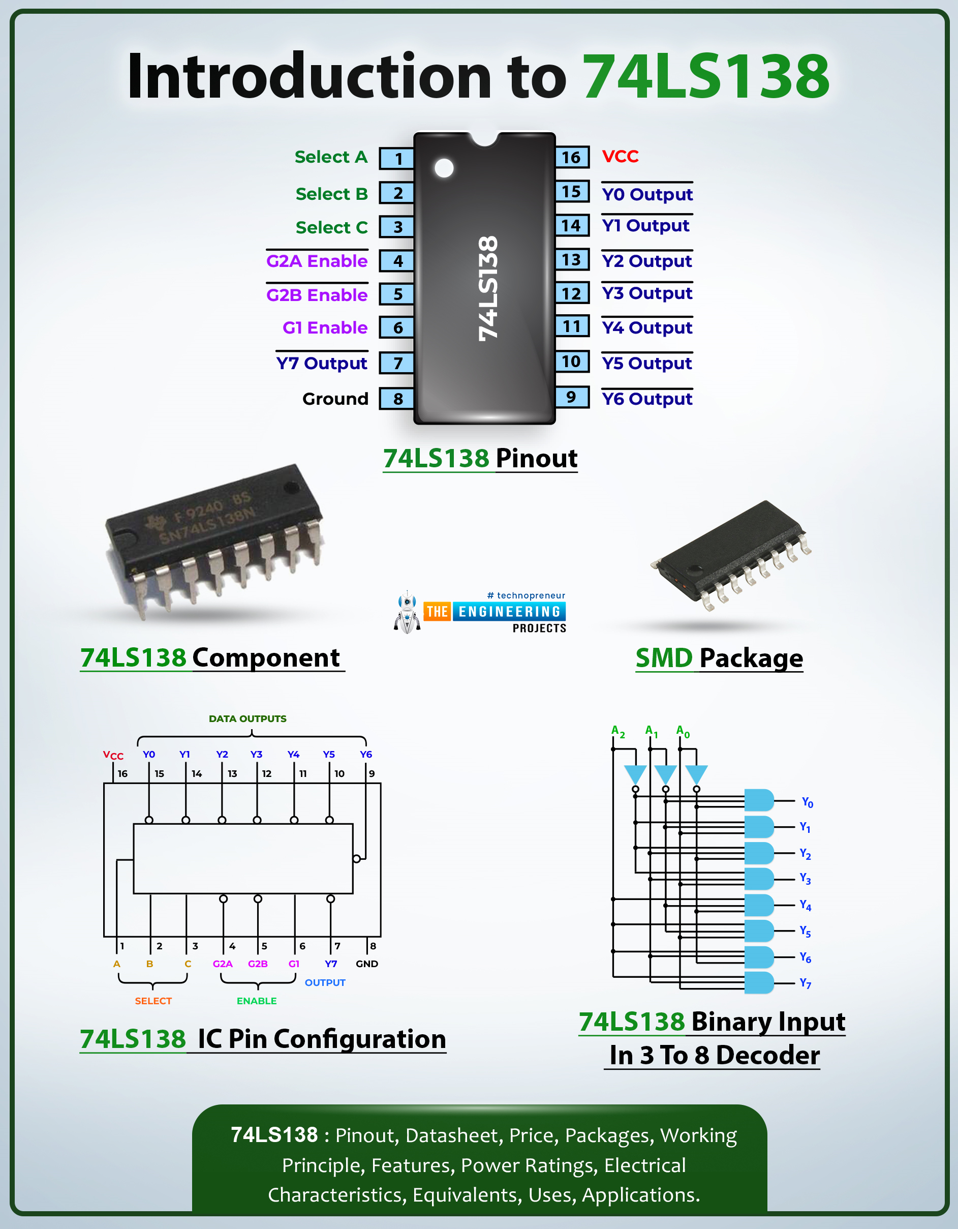
Features of 74LS138
The 74LS138 has the cascading feature which means, two or more 74LS138 can be connected together to enhance the number of output lines. The circuit is arranged in such a way that the output of one 74LS138 IC becomes the input of the other and as a result, more than one ICs can work together.
The structure of this IC is designed in such a way that it provides high-speed operation. It is done because the decoders are supposed to decode the input so quickly that its output may stimulate other functions of the circuits.
The TTL compatibility of the 74LS138 makes it more accurate. The LS in its name indicate that these are part of low-power shotkey series therefore, these can be operated at the 5V power supply. This makes it ideal for multiple electronic circuits and these do not require any additional device to get accurate power.
These ICs are versatile because they come in different packages and the users can have the right set of ICs depending on the circuit he is using. Two common packages of this IC are given next:
DIP (Dual Inline Package)
SOP (Small Outline Package)
It has multiple modes of operation therefore, it has versatile applications.
74LS138 IC Pin Configuration
Before using any IC in the circuit, it is important to understand its pinouts. The 73LS138 has the 16 pins structure that which is shown here:
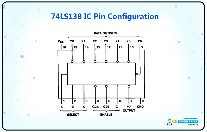
The detailed names and features of these pins can be matched with the table given below:

Pin Number |
Pin Name |
Pin Function |
1 |
A |
Address input pin |
2 |
B |
Address input pin |
3 |
C |
Address input pin |
4 |
G2A |
Active low enable pin |
5 |
G2B |
Active low enable pin |
6 |
G1 |
Active high enable pin |
7 |
Y7 |
Output pin |
8 |
GND |
Ground pin |
9 |
Y6 |
Output pin 6 |
10 |
Y5 |
Output pin 5 |
11 |
Y4 |
Output pin 4 |
12 |
Y3 |
Output pin 3 |
13 |
Y2 |
Output pin 2 |
14 |
Y1 |
Output pin 1 |
15 |
Y0 |
Output pin 0 |
16 |
VCC |
Power supply pin |
74LS138 in Proteus
The structure and working of this IC can be understood by creating a project with it and for this, we have chosen the Porteus to show the detailed working. Here are the steps to create the project of a 3 to 8 line decoder in Proteus:
Open your Proteus software.
Create a new project.
Go to the pick library by clicking the “P” button at the left side of the screen. It will show you a search box with details of the components.
Here, type 74LS138 and you will see the following search:

Double click on the IC to collect it on your devices.
Selecting this IC, click on the working sheet to place it there.

You can see the pins and labels of this IC.
Designing a 3 to 8 Line Decoder with 74LS138
The 74LS138 requires some additional components to be used as a decoder. Here is the project where we are using it as 3 to 8 line decoder:
Components Required
74LS138 IC
8 LEDs of different colors
Switch SPDT
Switch SPST
Switch Mom
Switch (simple)
Connecting wires
Procedure
Go to the pick library and get all the components of the circuits one after the other.
Set the 74LS138 IC in the working area.
On the left side of the IC, arrange the switches to be used as the input devices.
On the left side of the IC, arrange the LEDs that will indicate the output.
Go toto the terminal mode from the left side of the screen and arrange the ground and power terminals with the required devices.
The circuit at this point must look like the following image:

Connect all of these with the help of connecting wires. For convenience, I am using the labels to have better work:

Once you have connected all the components, the circuit is ready to use. In the left bottom corner, search for the play button and run the project.

Change the input with the help of switches and check for the output LEDs. You will see the circuit works exactly according to the truth table.
Working of 74LS138 IC in Proteus
The 74LS138 is designed to be used as a 3 to 8 line so there is no need to connect different ICs and components to design the working of this decoder.
The input and output pins are present with this IC therefore, the user simply connects the switches as an input device. A switch has only two possible states that are either on or off therefore, it is an ideal way to present the binary input.
Usually, LEDs are used as the output devices so that when they get the signal, they are turned on and vice versa.
The ground and power terminals are used to complete the circuit.
Pins 4, 5, and 6 are called the enabled pins. These are labeled as E1, E2, and E3 pins. Out of these, E1 and E2 are considered as the active low pins which means, these are active only when they are pulled down. On the other hand, the E3 is considered an active high; hence it activates the output only when it is pulled high.
Once the circuit is complete, the user can change the binary inputs through the switches and check for the output LEDs.
The combination of inputs results in the required output hence the user can easily design the circuit without making any technical changes.
Today, we have seen the details of 74LS138 decoder IC in Proteus. We started with the basic introduction of a decoder and saw what is the 3 to 8 line decoder isdecoder. After that, we saw the truth table and the features of a 3 to 8 line decoder. We saw how 74LS128 works and in the end, we designed the circuit of a 3 to 8 line decoder using 74LS138. The circuit was easy and we saw it working in detail. If you have any questions, you can ask in the comment section.


