Solder Paste Stencil Design: Essential for Perfect PCB Printing

Hi readers! I hope you are doing well and finding something new. In the high-speed world of electronics, a micrometer of solder paste can make or break your PCB assembly. Today, we will discuss solder paste stencil design and its importance for perfect PCB printing.
Solder paste stencil design is a building block of surface mount technology (SMT) and an important factor in the success of printed circuit board assembly (PCBA). The stencil is an exact template used for depositing solder paste onto PCB pads before the placement of components and soldering. Its design sets the amount of solder paste applied, its location, and how well it picks up from the stencil and gets onto the board. Even slight variations in stencil design can cause major assembly flaws, including solder bridging, inadequate solder joints, tombstoning of components, or improper alignment—all of which are factors in product reliability and manufacturing yield.
As contemporary electronics get smaller and more complex, the tolerance for error when applying solder paste is reduced. Perfect PCB printing involves keen attention to several stencil parameters such as material selection, aperture geometry, stencil thickness, area ratio, and surface finish. New age techniques such as nano-coating and step stencils have also improved performance for high-density and fine-pitch designs.
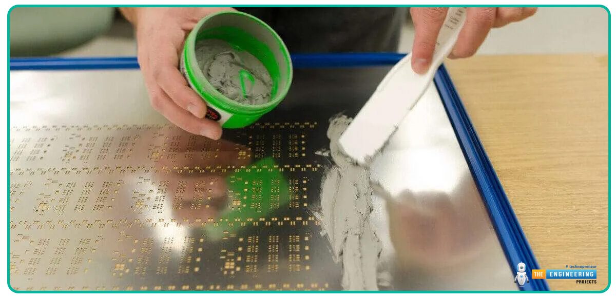
In this article, you will know the solder paste stencil, material used, manufacturing method, area ratio, aspect ratio, key stencil parameters, and common stencil-related defects and solutions. Let’s dive into the detailed guide.
Where can I order top-class PCBs online?
PCBWay Fabrication House has earned that initial trust as one PCB manufacturer. The firm has gained recognition for producing high-quality PCBs and solder paste stencils, as well as assembling at a considerably lower price than most. It offers simple 2-layer boards for highly complex flexible or high-frequency boards, which should sound as a recommendation for a wise move in both small and large orders. The process is easy: register, upload your Gerber files, fill in your board specifications, and get an instant quote. You can customize features like stencil manufacture and assembly before your order, and PCBWay does the rapid production and shipment around the globe. For orders and more inquiries, you can visit their website, mentioned below.
PCB fractures, such as copper trace cracks or layer delamination, can be caused by thermal stress, mechanical stress, or poor materials. PCBWay avoids this from happening by performing strict design reviews, utilizing high-quality materials, and precise stencil designs to make your PCBs robust and reliable for any application.
What is a Solder Paste Stencil?
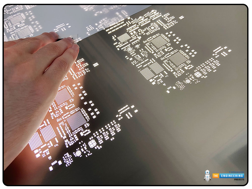
Basically, a solder paste stencil is a thin sheet of metal or polymer that has apertures chemically etched or laser-cut and formed into a copy of the solder pads on the PCB. The stencil is positioned on the surface of the PCB while the solder paste printing takes place through the openings of the stencil. The stencil avoids improper paste volume being deposited on every pad before component placement.
Importance of Stencil Layout in Solder Paste:
Impact on Solder Joint Strength:
Volume and the right positioning of solder paste can affect strong, defect-free joints. Less paste means just weak or incomplete joints, while too much leaves behind the problem of bridging, tombstoning, or cold solder joints. Optimization of the stencil layout ensures precise deposition of paste, eliminating all these common flaws.
Impact on Component Place Accuracy:
Proper solder paste volume guarantees that components settle onto their pads in the correct position before reflow. When the paste is uneven or less than ideal, components will lift or move, resulting in misalignment and poor connections. Consistent paste deposit allows for precise automated placement and robust mechanical bonding.
Impact on Reflow Performance:
Uniform solder paste deposits create uniform melting in the reflow step. Volume fluctuation in paste can cause overheating, voids, or solder balls, all of which jeopardize joint reliability. An ideal stencil design offers a uniform thermal profile and effective solder wetting.
Contribution to Yield and Reliability:
The repeatable stencil layout reduces manufacturing flaws, rework, and inspection expenses. Strong first-pass yield increases manufacturing productivity, and stable solder joints improve the long-term reliability of electronics products, grow customer satisfaction, and reduce warranty claims.
Stencil Materials and Manufacturing Methods:
Solder paste stencils are precious tools used in assembling PCB (Printed Circuit Board). They help in placing the right amount of solder paste at the right places on the board. Having the right stencil material and the right way to produce the stencil is critically important to get a good outcome. In this, we will outline common stencil materials, their benefits, and the process to produce the stencils.
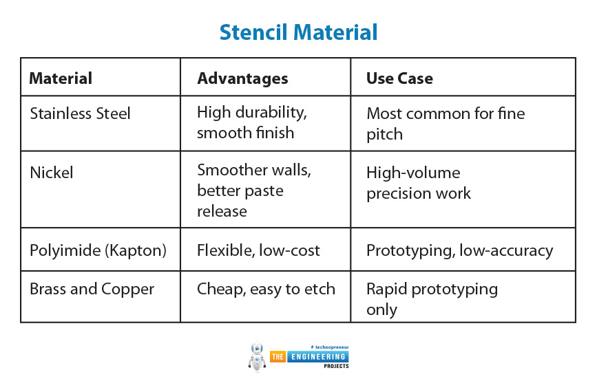
Stencil Material:
Material |
Advantages |
Use Case |
Stainless Steel |
High durability, smooth finish |
Most common for fine pitch |
Nickel |
Smoother walls, better paste release |
High-volume precision work |
Polyimide (Kapton) |
Flexible, low-cost |
Prototyping, low-accuracy |
Brass and Copper |
Cheap, easy to etch |
Rapid prototyping only |
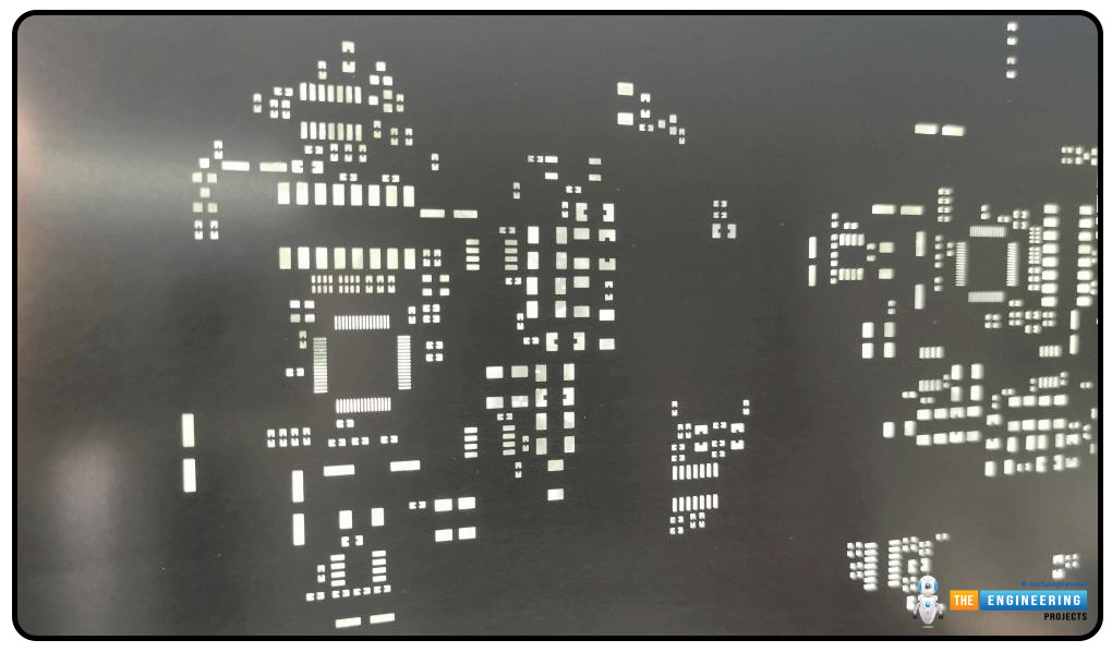
Stainless Steel:
The most common material used to make solder paste stencils is stainless steel. Stainless steel is very hard and durable. The stainless steel surface is smooth, and this makes it easy for the solder paste to release rapidly. Stainless steel stencils can be used for tiny and fine components on a PCB. Because of its hardness, it can be reused many times in small as well as in large production.
Nickel:
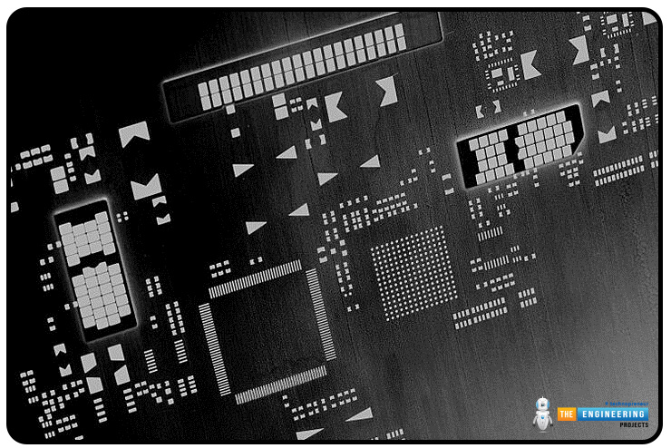
Nickel stencils are made using an electroforming process. Nickel stencils have very smooth edges, enabling solder paste to release cleanly from the stencil. Nickel stencils perform very well for high-volume production when there need to be accuracy. Nickel stencils are usually more expensive than stainless steel.
Polyimide (Kapton):
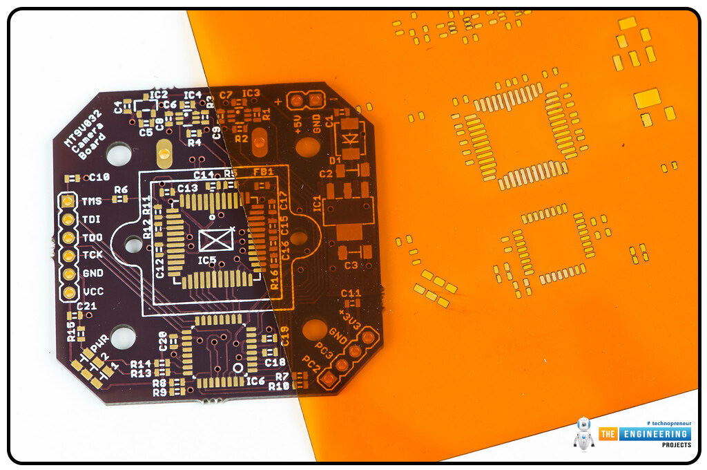
Polyimide, or Kapton, is a pliable, cheaper-than-metal stencils plastic-like material. It is used most frequently for proof-of-concept or testing PCB designs. Since it is flexible, it may be put on surfaces that are not flat. However, polyimide stencils wear out faster and are less accurate than metal stencils.
Brass and Copper:
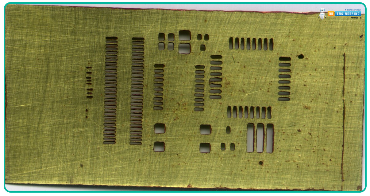
Brass and copper stencils are inexpensive and easy to manufacture using etching. Because of their low costs, they are used mostly in the rapid prototyping process. These materials, however, are soft and don't last long. They aren't suitable for fine-pitch devices and bulk production runs.
Fabrication Techniques:
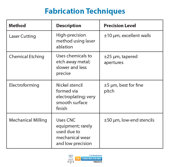
Method |
Description |
Precision Level |
Laser Cutting |
High-precision method using laser ablation |
±10 µm, excellent walls |
Chemical Etching |
Uses chemicals to etch away metal; slower and less precise |
±25 µm, tapered apertures |
Electroforming |
Nickel stencil formed via electroplating; very smooth surface finish |
±5 µm, best for fine pitch |
Mechanical Milling |
Uses CNC equipment; rarely used due to mechanical wear and low precision |
±50 µm, low-end stencils |
Laser Cutting:
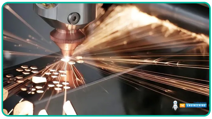
Laser cutting is the most common way of producing solder paste stencils. A laser beam accurately cuts small holes in the stencil material. Laser cutting can produce extremely small hole sizes, usually about 10 microns (a micron is one millionth of a meter). The edges of the holes are straight, which helps in the release of solder paste. Laser cutting is fast and accommodates most PCB designs.
Chemical Etching:
Chemical etching uses chemicals to remove parts of the stencil material once it has been covered with a specific pattern. It is less precise and slower than laser cutting, with average accuracy around 25 microns. The holes created by etching are slightly tapered, and this can affect how solder paste sticks and releases. It is mostly used with easier or less expensive stencils.
Electroforming:
Electroforming is a special process of plating nickel on a patterned surface to generate very fine and smooth stencil holes. It is the most accurate, with an accuracy of up to 5 microns. Electroformed stencils are most suitable for very small and fragile PCB components, but they cost more and take more time to produce.
Key Stencil Parameters:
Stencil Thickness:
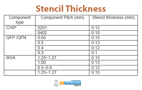
Typical stencil thickness can be anywhere from 0.10 mm to 0.20 mm, where the selection usually depends greatly on component size and pitch.
0201 and 01005 Passive Components:
Owing to the fine deposits of these tiny components' solder paste, a 0.10 mm to 0.12 mm thin stencil should be employed. This helps to minimize the chances of paste smearing or excessive solder volume that would lead to bridging or tombstoning.
QFNs (Quad Flat No-leads) and Fine-Pitch BGAs (Ball Grid Arrays):
These are liable to feature fine-pitch leads or thermal pads, which must undergo controlled paste deposition to prevent floating or inadequate solder coverage. A nominally thicker 0.12 mm to 0.15 mm stencil provides adequate volume without sacrificing accuracy.
0603 and 0805 Passives:
The thickness for these mid-range devices is normally in the 0.15 mm to 0.18 mm range. The thickness provides a sufficient volume of solder paste to provide adequate mechanical and electrical bonding without an unacceptably high risk of bridging.
Connectors and LGAs (Land Grid Array):
Larger devices tend to need a larger volume of solder paste, and therefore, 0.18 mm to 0.20 mm thickness is satisfactory.
Aperture Design:
Standard aperture shapes are mentioned below.
Rectangular:
Widely used passive component shapes for resistors and capacitors. Comparable shape to rectangular pads and permits uniform paste transfer.
Rounded Rectangle:
Rounded corners and edges, which have the added benefit of dispensing solder paste off the stencil with reduced possibility of paste getting trapped in acute corners. Rounded rectangles minimize the risk of smearing paste and provide improved print consistency.
Home Plate:
The shape is inverse trapezoidal. Home plate openings are utilized in an attempt to minimize tombstoning, a sort of flaw whereby one end of the chip components becomes lifted upon reflow because there have been irregular amounts of solder paste. Solder is diminished by the aperture in the component's ends, and symmetry is created for paste deposition within improved mechanical stability.
Circular:
Frequently used for BGAs and in-pad via packaging, circular apertures feature symmetrical ball and via deposits. In the case of fine-pitch BGAs, controlled aperture diameter and spacing in circular apertures eliminate solder bridging and enhance the joint reliability.
Area Ratio and Aspect Ratio:
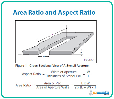
These two ratios are vital for ensuring adequate paste release.
4.1 Area Ratio (AR):
AR=Aperture AreaAperture Wall Area=WL2(W+L)T
Where:
W = aperture width
L = aperture length
T = stencil thickness
AR ≥ 0.66 is ideal for good paste release.
4.2 Aspect Ratio:
Aspect Ratio=Aperture WidthStencil Thickness
Recommended > 1.5 to avoid paste clogging or incomplete prints.
Stencil Design Best Practices:
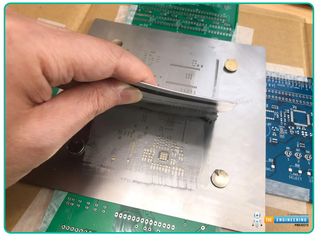
Fiducials and Alignment:
Always include global and local fiducials.
Ensure fiducials are clear of solder mask and have sufficient clearance from pads.
Paste Reduction Techniques:
Use step-down stencils where different component groups require different paste volumes.
Apply nano-coating on the stencil to enhance paste release and reduce cleaning frequency.
Stencil Frame Types:
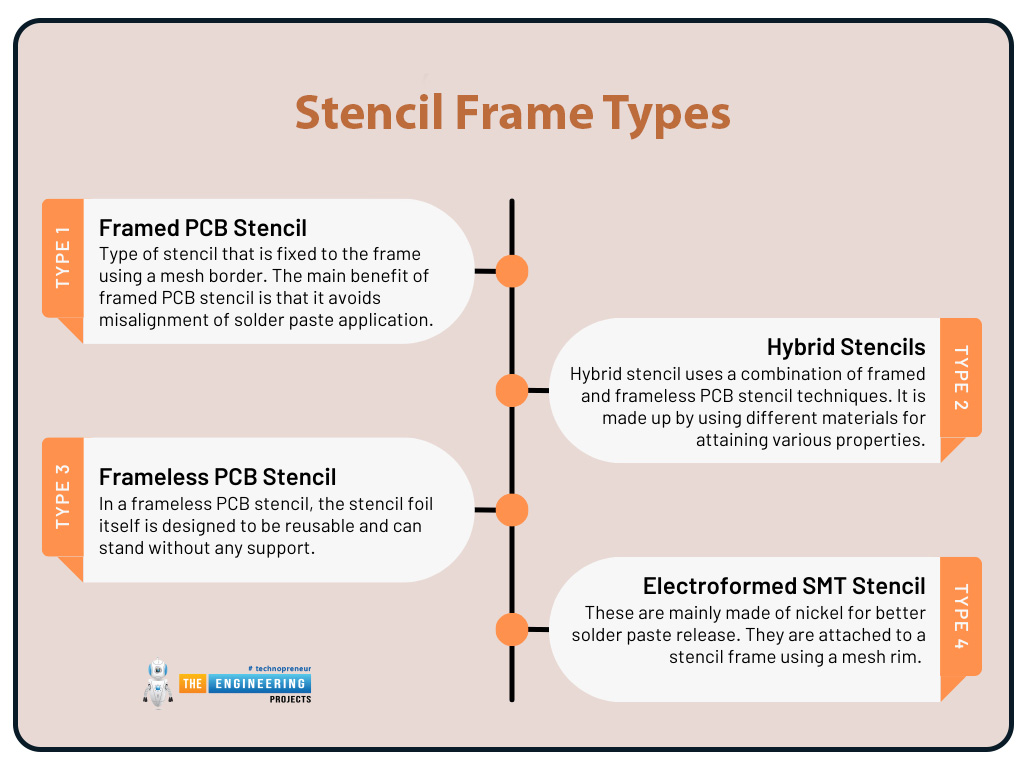
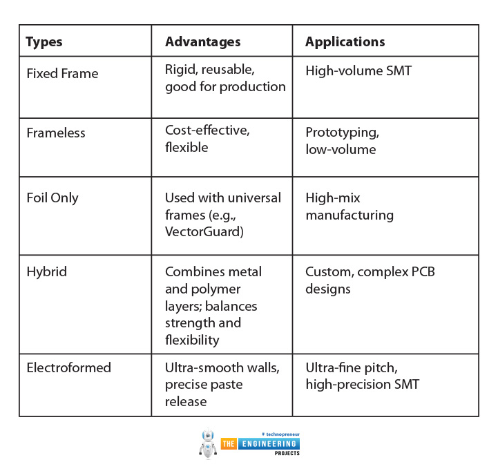
Types |
Advantages |
Applications |
Fixed Frame |
Rigid, reusable, good for production |
High-volume SMT |
Frameless |
Cost-effective, flexible |
Prototyping, low-volume |
Foil Only |
Used with universal frames (e.g., VectorGuard) |
High-mix manufacturing |
Hybrid |
Combines metal and polymer layers; balances strength and flexibility |
Custom, complex PCB designs |
Electroformed |
Ultra-smooth walls, precise paste release |
Ultra-fine pitch, high-precision SMT |
Common Stencil-Related Defects and Fixes:
Defect |
Cause |
Solution |
Solder Bridging |
Excessive paste, poor aperture design |
Reduce aperture size, optimize AR |
Insufficient Solder |
Small apertures, worn stencil, poor squeegee angle |
Use a thicker stencil or redesign |
Tombstoning |
Imbalanced paste volume across pads |
Use home plate apertures |
Smeared Prints |
Dirty stencil, low squeegee pressure |
Clean stencil, adjust pressure |
Misalignment |
Poor fiducials or stencil placement |
Improve alignment features |
Conclusion:
Stencil design for solder paste preparation is not merely making holes in a stainless steel sheet; it is an involved engineering task and is the basis for successful surface mount technology (SMT) assembly. The stencil controls how much solder paste is applied and where it is applied, and how uniformly it distributes it; hence has a lot of effect on product quality and manufacturing yield.
The design of a stencil should consider a complete interplay between freedom of aperture geometry, stencil thickness, and other areas, aspect ratio, and material selection. All the above parameters need to be calibrated with the respective components and PCB layout to guarantee that faults such as bridging, tombstoning, under solder, and misalignment are eliminated.
Implementing best practices such as using home plate apertures for chip components, nano-coating to improve paste release, and following standard cleaning and inspection procedures further enhances stencil performance and print quality.
Since assemblies are more dense and components are smaller, stencil design accuracy becomes necessary in place of being desirable. For engineers and PCB manufacturers requiring high-quality, blemish-free PCB prints, solder paste stencil design is a vital skill involved in the process.


