What is Microvia Technology? Used for Miniaturization in Modern PCBs

Hi readers! Hopefully, you are having a great day and exploring something new and advanced. In the competition to miniaturize electronics and increase performance, the smallest holes in your PCB, micro vias, are carrying the biggest load. Today, the topic of our discourse is micro via technology and its use for miniaturization in modern PCBs.
In this electronic revolution, the thirst for miniaturization, speed, and power will remain insatiable. Today's electronics scale down, complexity increases daily, from smartphones to wearable devices, from aerospace equipment to medical implants. Behind this miniaturization process is a key breakthrough in printed circuit board (PCB) technology, Microvia Technology.
Microvias are extremely small vias, usually under 150 microns in diameter, for connecting layers of high-density interconnect (HDI) PCBs. Microvias are different from the normal through-hole vias that extend the entire thickness of the board; microvias are laser-drilled and frequently connect only adjacent layers. The designers can thus maximize usable board area, route more signals in less space, and enhance electrical performance without increasing overall size and weight.
With increasingly dense and layered electronic designs, conventional methods of interconnection are no longer sufficient to deal with the constraints of speed, size, and reliability. The problem is fixed by microvia technology, allowing for multi-layer interconnection within very tight packages without sacrificing integrity or signal integrity. Microvia technology is essential to facilitate state-of-the-art HDI PCB configurations and, today, the key to modern electronic design.
In this article, we’ll explore what microvia technology is, how it works, why it is essential for modern electronics, its role in shrinking PCBs, and its applications. Let’s start.
Where to Buy PCBs Online? Choose PCBWay, Preferred by Engineers Globally
If you need to buy printed circuit boards (PCBs) online, PCBWay is among the top options. If you are a student, hobbyist, or professional engineer, or something else, PCBWay makes it easy for you to get top-quality PCBs produced just as you want them. Upload your design files, receive an instant price quote, and place an order all with just a few clicks. They ship PCBs quickly and deliver worldwide.
PCBWay is also very reliable and affordable. They can manufacture all types of boards from low-profile two-layer PCBs to high-profile multilayer boards using special materials such as high-frequency Rogers and flexible circuits. Their team inspects your files for errors prior to production and provides useful recommendations, which saves both time and money.

One amazing aspect of PCBWay is their rapid prototyping service. If you're short on time and want your PCB quickly to test or use in a project, they will produce and send it to you in a minimum of 24 hours! This is ideal for individuals who need to build and test something in a hurry. With excellent customer support and quality, PCBWay is an intelligent choice to order your next PCB.
What is Microvia Technology?
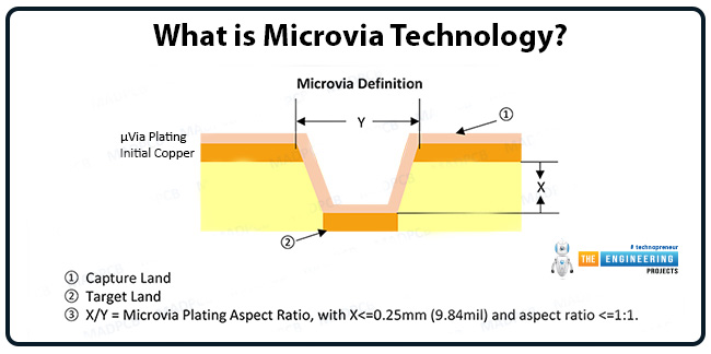
Microvia technology requires making very fine connections using small, laser-punched holes called Microvias in printed circuit boards (PCBs). Microvias are used to interconnect neighboring layers on a PCB and have a diameter of less than 150 microns. Requiring far smaller diameters than conventional vias, Microvias will impact only one or two layers rather than the entire board, so much higher circuit density can be achieved. Microvia technology provides the capability for High-Density Interconnect (HDI) PCBs, allowing for the creation of smaller, quicker, and more complicated electronic devices. Microvia technology provides the capability for routing space and signal integrity to enhance the performance of a PCB. Microvia technology is thus a major facilitator of today's miniaturization and evolution of numerous electronic products, such as smartphones and wearables.
Key Microvia Characteristics:
1. Diameter:
Microvias are below 150 µm (0.15 mm) in diameter. Microvias can fit very little space on the PCB due to their small size, which is a critical factor in high-density design where micron is a critical factor.
2. Depth:
A representative depth ranges from 50 to 100 µm, just deep enough to connect adjacent layers without introducing mechanical stress or affecting board reliability.
3. Aspect Ratio:
Microvias are built to an aspect ratio (depth-to-diameter) of 1:1 or less. A lower aspect ratio improves plating quality and structural integrity and reduces the risk of defects like cracks or voids.
4. Fabrication Method:
Microvias are laser-drilled, either with CO₂ or UV lasers. Laser drilling provides very high accuracy and eliminates mechanical drilling's wear and size limitations.
5. Layer Connection:
Microvias usually connect adjacent layers, Layer 1 to Layer 2. Limited depth provides signal integrity and board strength, and makes stacked or staggered via structures possible in deep HDI boards.
6. Thermal Reliability:
Microvias provide thermal reliability since they are shallow in depth and subject to minimum copper plating stress. Stacking or plating failure would cause failure, hence, proper process control must be applied during HDI production.
7. Signal Integrity:
Their compact size and low parasitic capacitance make microvias suitable for high-speed signal transmission. They reduce signal loss and distortion, which is critical in RF, high-frequency, and digital designs.
8. Space Optimization:
Microvias allow for high-density component placement and tighter routing, especially under BGA and CSP (Chip Scale Package) packages. This allows for smaller PCBs without sacrificing performance.
9. Design Flexibility:
Because microvias are constrained to interconnect adjacent layers, they offer new routing potential, especially when applied with HDI stack-ups like 1+n+1 or 2+n+2 (where "n" equals the number of core layers). This offers greater flexibility in layer design and signal flow.
Types of Microvias:
Microvias can be categorized based on their structure and interconnect method:
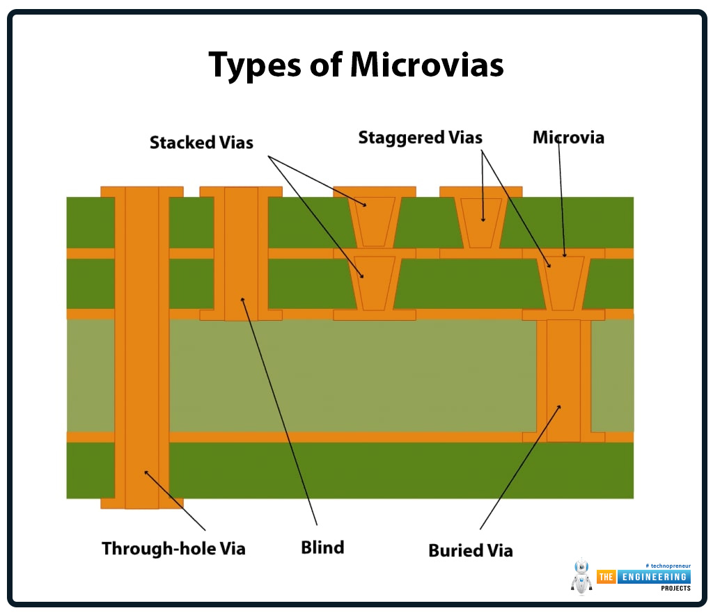
Blind Microvias:
Connect an outer layer to an inner layer
Do not pass through the entire board
Ideal for freeing up surface real estate
Buried Microvias:
Connect two or more inner layers
Not visible from outer layers
Used when blind vias and through-holes are insufficient
Stacked Microvias:
Created by stacking multiple blind or buried microvias
Common in advanced HDI designs with more than 8 layers
Staggered Microvias:
Microvias offset across layers rather than being stacked vertically
Reduces stress buildup and improves reliability
Skip Microvias:
Connect non-adjacent layers by “skipping” an intermediate one
More challenging to fabricate; used sparingly
Microvia Fabrication Process:
Creating microvias involves several critical steps:
Sequential Lamination:
The process begins by laminating a core with dielectric material. Additional layers are built up using sequential lamination, where each new layer is drilled and metallized before the next is added.
Laser Drilling:
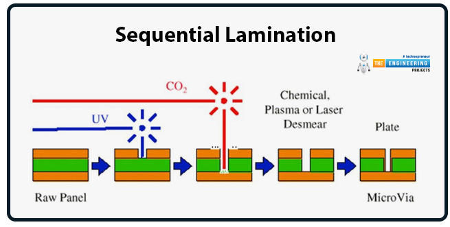
UV or CO₂ lasers drill precise, conical holes in the dielectric.
UV lasers offer finer resolution and are preferred for very fine features.
Laser parameters must be optimized to prevent resin recession and debris.
Desmearing:
Chemical or plasma cleaning removes carbonized resin from the via walls to ensure clean metallization.
Electroless and Electrolytic Plating:
The vias are metallized by depositing a thin seed layer, followed by copper electroplating to ensure conductivity.
Filling and Capping:
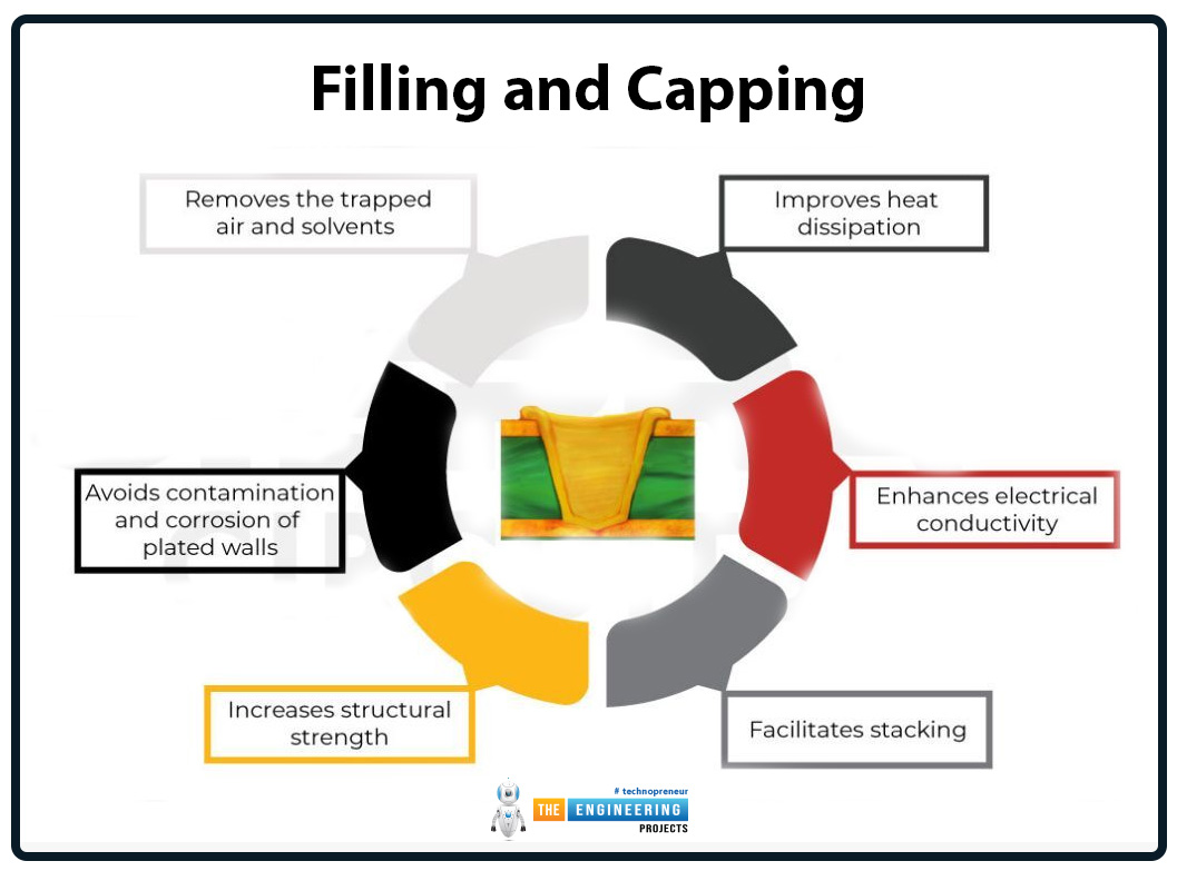
Copper filling is often used for stacked microvias to maintain structural integrity and avoid voids.
Planarization ensures a flat surface before the next lamination cycle.
Design Guidelines for Microvias:
Designing for microvia technology requires precision and adherence to manufacturing constraints:
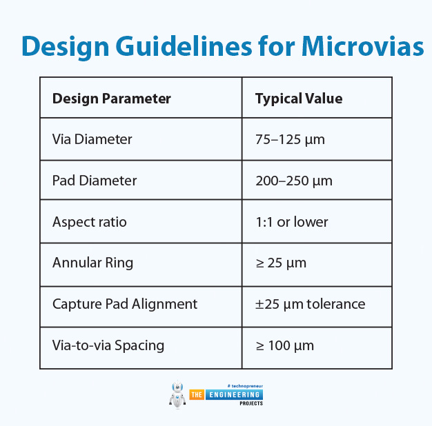
Design Parameter |
Typical Value |
Via Diameter |
75–125 µm |
Pad Diameter |
200–250 µm |
Aspect ratio |
1:1 or lower |
Annular Ring |
≥ 25 µm |
Capture Pad Alignment |
±25 µm tolerance |
Via-to-via Spacing |
≥ 100 µm |
Key Design Tips:
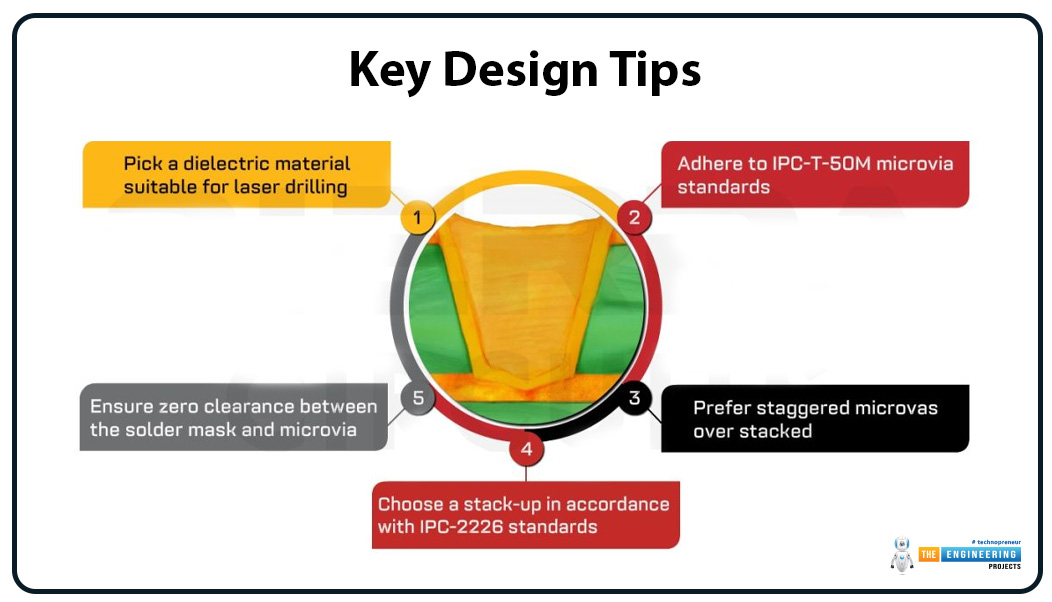
Maintain proper aspect ratio to ensure reliable plating.
Use staggered rather than stacked microvias where possible for better yield.
Account for drill tolerance and registration accuracy when assigning pad sizes.
Keep thermal expansion and Z-axis stress in mind for multilayer stacks.
The Role of Microvia Technology in Shrinking PCB Sizes:
The modern electronics business is defined by an insatiable demand for smaller, quicker, and more efficient devices. It may be smartphones, tablets, fitness wearables, medical implants, or autonomous vehicle technology; manufacturers are constantly fighting the battle of squeezing more performance into increasingly smaller housings. Traditional PCB technology can't keep pace with these demands. That is where microvia technology comes in, enabling engineers to create high-density interconnect (HDI) PCBs that fit in as much component placement and routing density as possible without expanding board size. The way microvias shrink PCBs is mentioned below.
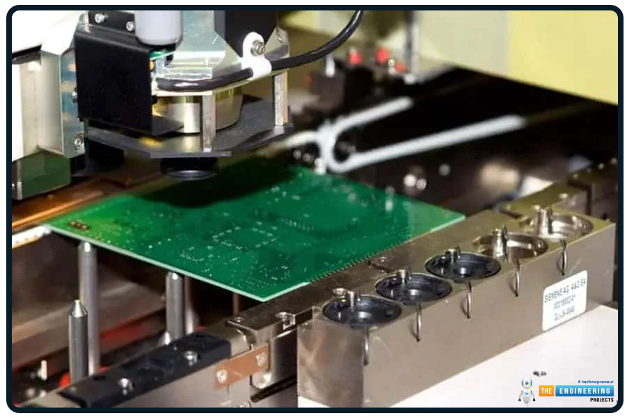
Space Efficiency and Routing Density:
Because microvias occupy less surface area on both the surface and inner layers, they allow more signal traces to be routed per square inch of board space. This is particularly important for devices using fine-pitch BGAs or chip-scale packages (CSPs), where space is highly constrained. Designers can position vias underneath these packages without disrupting close traces, virtually occupying the entire PCB real estate. This efficiency promotes more functionality without increasing board size, thus making microvias critical in miniaturization.
Advanced Layer Connections:
Microvias are not used alone; microvias can be made into complex structures, including:
Stacked Microvias: Vertically stacked microvias that connect multiple layers in a linear path.
Staggered Microvias: Offset microvias that connect layers in a zigzag manner, offering greater mechanical strength.
Via-in-pad: This is where via-in-pad microvias are usually located under the pad of a component that is commonly used in high-density BGA designs.
Taking advantage of these structures, therefore, improves routing flexibility and ultimately enables stacking of components and signals vertically, thereby greatly improving the efficiency of board design.
Better Electrical Performance:
Microvias are said to have much better electrical performance than through-hole connections, especially from high-speed and high-frequency devices. Due to their small size, these inductors tend to have parasitic inductance and capacitance, thus cleaner signal transmission with fewer signal losses. This extra quality makes microvia-based PCBs particularly favorable for 5G, high-speed DDR memory, and RF-based communications devices, as these also help reduce signal skew and crosstalk that are critical in multilayer, high-speed environments.
Precision Manufacturing with Laser Drilling:
Microvias are fabricated through high-accuracy laser drilling, typically with CO₂ or UV lasers. Microvias generate clean hole creation without mechanical strain on the adjacent material. After drilling, holes are copper plated with electroplating or direct metalization, establishing strong interlayer interconnections. Depth and diameter control are vital to ensure plating quality, structural integrity, and reliability in the long term.
Applications of Microvia Technology:
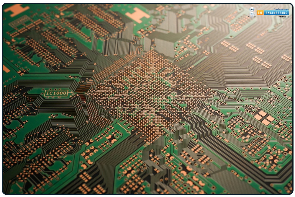
Space Efficiency: Ideal PCB Real Estate Optimization
Microvias significantly minimize the space needed for vertical interconnection among layers of a PCB. This makes room for more circuitry to be accommodated in smaller board areas, enabling the creation of compact and light electronic devices.
High-Density Layer Stacking:
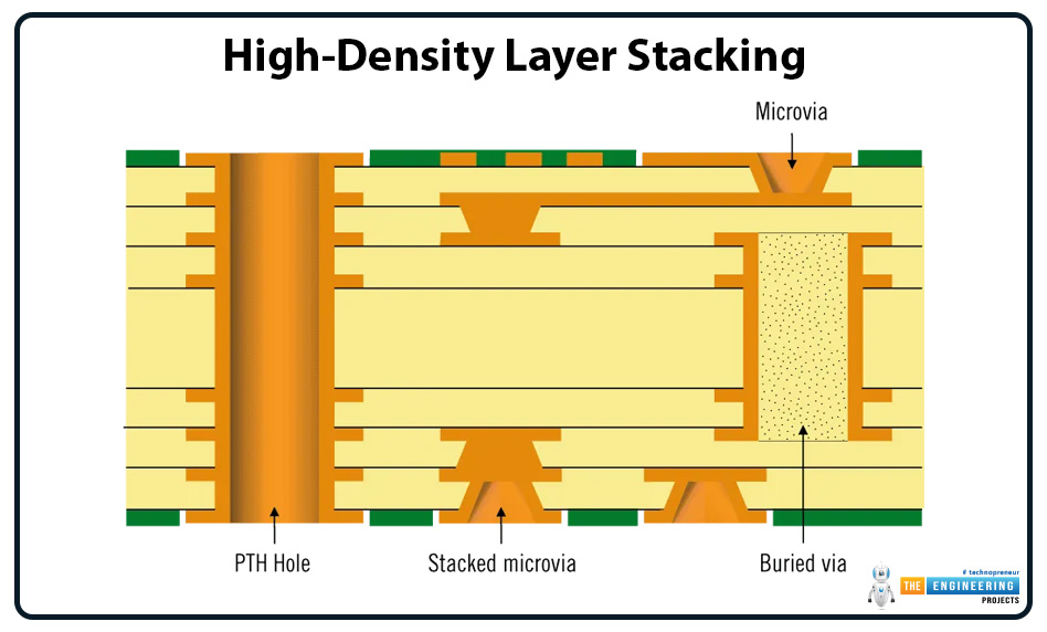
Since microvias are only between adjacent layers, they allow for having numerous layers in a multilayer PCB without really adding much thickness and size. This leads to smaller overall PCB footprints.
Improving Signal Integrity:
As the electrical lengths that are reduced translate directly to signal losses, which are lost to overheating in electromagnetic interference, microvias restrict the crossover of traces. Data transmission is cleaner and faster, a specialty in high-speed electronics.
Improving Electrical Performance:
By minimizing parasitic capacitance and inductance, microvias provide higher frequency performance and enhanced overall electrical performance, crucial for today's communications and computing hardware.
Mechanical Reliability: Minimization of Stress Points
Microvia's smaller size and accurate placement minimize mechanical stress in the PCB structure, lowering the risk of cracking or delamination with thermal cycling and mechanical shock.
Thermal Management Benefits:
Microvias enable increased heat dissipation via the PCB layers, lowering component temperatures and enhancing device life and reliability.
Widely Applied in Most Industries:
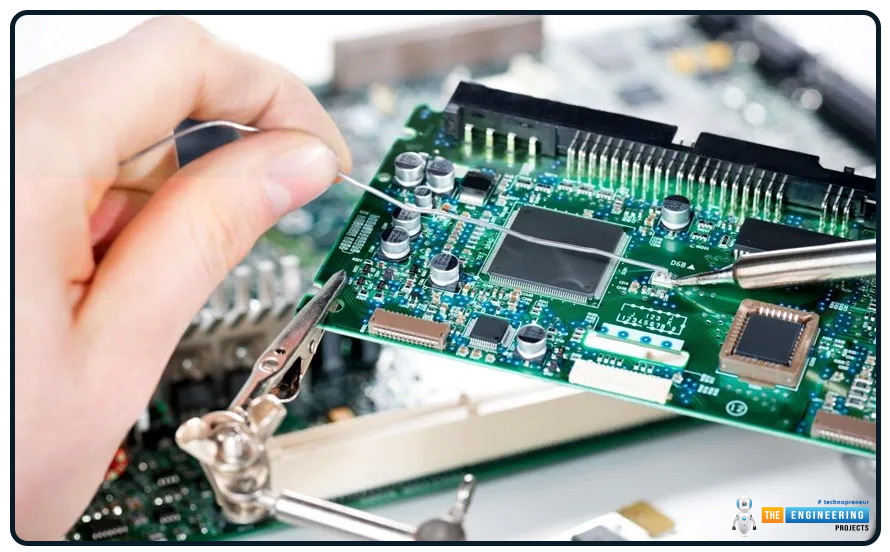
Due to these advantages, microvia technology is widely applied in consumer electronics (smartphones, tablets), automotive (ADAS systems), aerospace (avionics), medical devices (pacemakers), telecom (5G equipment), and industrial automation (sensors and controllers).
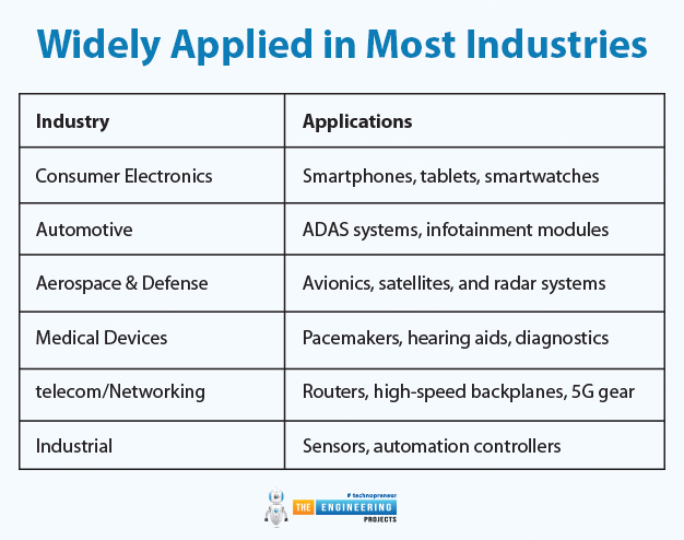
Industry |
Applications |
Consumer Electronics |
Smartphones, tablets, smartwatches |
Automotive |
ADAS systems, infotainment modules |
Aerospace & Defense |
Avionics, satellites, and radar systems |
Medical Devices |
Pacemakers, hearing aids, diagnostics |
telecom/Networking |
Routers, high-speed backplanes, 5G gear |
Industrial |
Sensors, automation controllers |
Conclusion:
Microvia technology is the backbone of contemporary PCB miniaturization, allowing small, high-performance, and reliable board fabrication. With decreasing size and increasing sophistication of electronic products, conventional through-hole vias cannot meet the demands for closer density and improved signal integrity. Microvias provide the solution to this challenge by allowing the potential to manufacture complex high-density interconnect (HDI) designs with finer pitches and greater routing density.
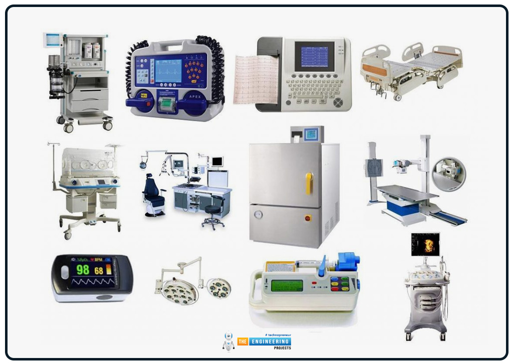
Though more expensive and technically demanding than traditional via fabrication, the advantages are worth it in today's electronics. Microvia technology, previously the prerogative of premium systems, is used extensively in consumer electronics, industrial equipment, and healthcare systems.
The future of PCB design will be focused on the evolution of microvia technology, and this technology will be employed to support even greater integration, reduced feature size, and components embedded inside. Microvias will need to be learned by both PCB designers and manufacturers to remain at the forefront of the rapidly changing world of electronics. Microvias will remain an engine for smaller, faster, and more efficient electronic products as technology continues to evolve.


