Introduction to PIC16F877

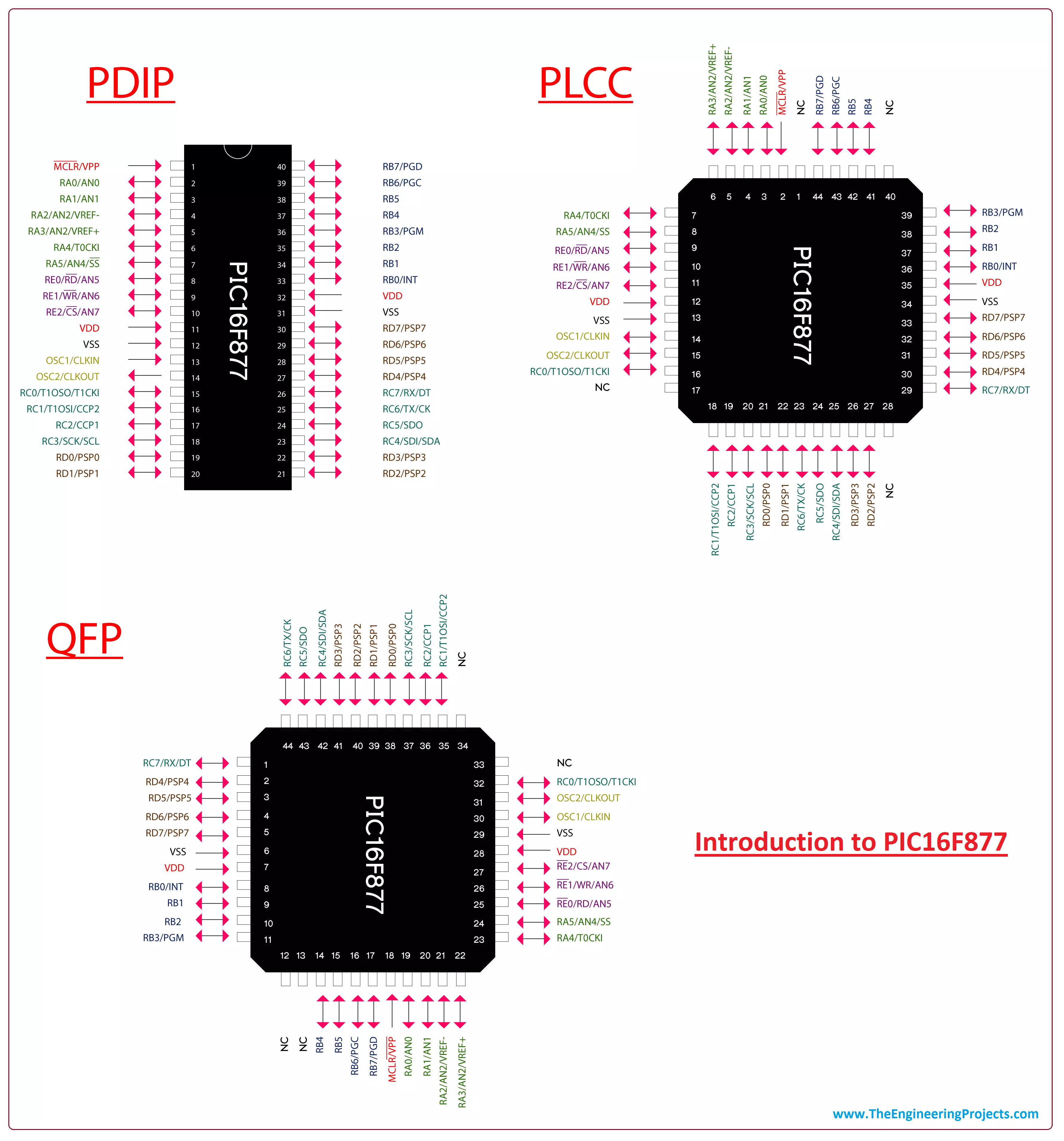
Hey Guys! Hope you are doing well. I am back to give you valuable information as per your technical needs and requirements. Today, I’ll unlock the detailed Introduction to PIC16F877. It is an 8-bit PIC microcontroller that comes with 40-pin interface (PDIP). It is based on Flash type memory. The High-Performance RISC CPU is incorporated inside the device that comes with only 35 single-word instructions, targeting mainly two types of instructions: single cycle and double-cycle. In this post, I'll cover each and everything related to PIC16F877: its features, pinout and pin description, main functions, memory interface, compiler and burner used and applications. Let's dive right in and get down to the nitty-gritty of this tiny device.

Introduction to PIC16F877

  • PIC16F877 is an 8-bit PIC microcontroller that is introduced by Microchip and is mainly used in automation and embedded systems.
It comes in three packages known as PDIP, PLCC, and QFN where the first one is 40-pin while other two come with a 44-pin interface.
  • It features 256 bytes of EEPROM data memory, 368 bytes of RAM, and program memory of 14K.
This microcontroller version incorporates CPU, timers, 10-Bit ADC and other peripherals that are mainly used to develop a connection with external devices.
  • The decent memory endurance around 1,000,000 for EEPROM and 100,000 for program memory, makes this device an ideal choice for many real-time applications.
The Universal Synchronous Asynchronous Receiver Transmitter (USART) is very helpful for developing serial communication with other devices.
  • Some internal and external reset features are added in the device that prevents the device from going stale, giving you a full authority to modify the controller as per your needs and requirements.
If automation is anything to go by, you cannot write off the importance of this little toy.

1. PIC16F877 Features

You have got a brief overview of the device. In this section, I have arranged the main features in a single table, making it easy for you to grab the main idea about the device. Let's have a look at the table.
CPU PIC
CPU Size 8-Bit
Total Number of Pins 40
I/O Pins 33
Analog Input 6
Flash Memory (Program Memory) 14 KB
SRAM 368 Bytes
EEPROM 256 Bytes
Timers (3) Timer0 Timer1 Timer2
Operating Voltage 4 to 5.5 V
Oscillator (Speed) up to 20 MHz
Manufacturer Microchip
Number of Ports (5) PORTA PORTB PORTC PORTD PORTE
Instruction Set 35 instructions
Capture/Compare/PWM Modules 2
Interrupts 14
A/D Converter 10-bit, 8 Channel
BOD (Brown Out Detection) Yes
Watch Dog Timer Yes
UART (Serial Communication) Yes
SPI Protocol Yes
I2C Protocol Yes
ICSP (In Circuit Serial Programming) Yes
DC Current for 3.3V Pin 50 mA
  • These features will help you understand the main characteristics of the controller and guide you in making a final decision before you intend to incorporate this chip into a certain project.

2. PIC16F877 Pinout and Description

In this section, we cover the pinout of the controller and a detailed description of each pin.
PIC16F877 Pinout
Following figure shows the pinout of PIC16F877.
  • This module comes in three packages known as  PDIP, PLCC, and QFP. The first one is mainly used for developing individual projects while other two are widely used in industrial applications.
PIC16F877 Pin Description
Following table shows the pin description of each pin. Some pins are capable to perform more than one function.
Pin# Pin Name Pin Description
1 MCLR' VPP Master Clear Active Low Reset Pin ICSP Programming Enable Pin
2 RA0 AN0 Digital I/O Pin Analog Input 0 Pin
3 RA1 AN1 Digital I/O Pin Analog Input 1 Pin
4 RA2 AN2 VREF- Digital I/O Pin Analog Input 2 Pin ADC Reference Input Voltage (low)
5 RA3 AN3 VREF+ Digital I/O Pin Analog Input 3 Pin ADC Reference Input Voltage (high)
6 RA4 T0CKI Digital I/O Pin External clock input for Timer0
7 RA5 AN4 SS' Digital I/O Pin Analog Input 4 Pin Slave Select input for SPI
8 RE0 AN5 RD' Digital I/O Pin Analog Input 5 Pin Read control for the parallel slave
9 RE1 AN6 WR' Digital I/O Pin Analog Input 6 Pin Write control for the parallel slave
10 RE2 AN7 CS' Digital I/O Pin Analog Input 7 Pin Select control for the parallel slave
11 VDD Voltage Supply Pin
12 VSS Ground Pin
13 OSC1 CLKIN Crystal Oscillator Input Pin
14 OSC2 CLKOUT Crystal Oscillator Output Pin
15 RC0 T1OSO T1CKI Digital I/O Pin Oscillator output for Timer1 External clock input for Timer1
16 RC1 T1OSI CCP2 Digital I/O Pin Oscillator input for Timer1 Output for Compare2 and PWM2, Input for Capture2
17 RC2 CCP1 Digital I/O Pin Output for Compare1 and PWM1, Input for Capture1
18 RC3 SCK SCL Digital I/O Pin SPI Module Synchronous serial clock input/output I2C Module Synchronous serial clock input/output
19 RD0 PSP0 Digital I/O Pin Parallel Slave Port for D0 with TTL input buffers
20 RD1 PSP1 Digital I/O Pin Parallel Slave Port for D1 with TTL input buffers
21 RD2 PSP2 Digital I/O Pin Parallel Slave Port for D2 with TTL input buffers
22 RD3 PSP3 Digital I/O Pin Parallel Slave Port for D3 with TTL input buffers
23 RC4 SDI SDA Digital I/O Pin SPI Data-In Pin I2C Data I/O Pin
24 RC5 SDO Digital I/O Pin SPI Data-Out Pin
25 RC6 TX CK Digital I/O Pin Asynchronous Transmit (USART) Synchronous Clock (USART)
26 RC7 RX DT Digital I/O Pin Asynchronous Receive (USART) Synchronous Data (USART)
27 RD4 PSP4 Digital I/O Pin Parallel Slave Port for D4 with TTL input buffers
28 RD5 PSP5 Digital I/O Pin Parallel Slave Port for D5 with TTL input buffers
29 RD6 PSP6 Digital I/O Pin Parallel Slave Port for D6 with TTL input buffers
30 RD7 PSP7 Digital I/O Pin Parallel Slave Port for D7 with TTL input buffers
31 VSS Ground Pin
32 VDD Voltage Supply Pin
33 RB0 INT Digital I/O Pin External Interrupt 0
34 RB1 Digital I/O
35 RB2 Digital I/O
36 RB3 PGM Digital I/O ICSP programming enable pin (Low voltage)
37 RB4 Digital I/O
38 RB5 Digital I/O
39 RB6 PGC Digital I/O ICSP programming clock, In-circuit debugger
40 RB7 PGD Digital I/O ICSP programming data, In-circuit debugger

3. PIC16F877 Main Functions

This PIC model is capable to perform many functions similar to other controllers in the PIC family. Following are the main functions of PIC16F877.
Timer
PIC16F877 comes with three timers known as Timer0 (8-bit), Timer1(16-bit) and Timer2 (8-bit). These timers can be used as a timer as well as a counter.
  • The timer mode is mainly used to increment the instruction cycle while the counter mode plays a vital role to increment the rising and falling edge of the pin.
All three timers contain internal and external clock select capability.
USART
PIC16F877 incorporates a USART (Universal Synchronous and Asynchronous Receiver and Transmitter) module that is mainly used to establish the serial communication with external devices.
Watchdog Timer
PIC16F877 comes with a built-in watchdog timer that takes the controller back to reset position if the program hangs up during compilation or gets stuck in the infinite loop.
  • It is nothing but a hardware timer that produces a system reset if the main program fails to periodically service it.
It is advised to reset this timer to the initial value after every 3 instructions in order to avoid it going to zero value in normal conditions.
  • The Watchdog Timer can be controlled only through configuration bits. It comes with its own RC oscillator for maximum reliability.
Brown Out Reset (BOR)
The BOR function is a very remarkable addition that puts the device in reset condition once the Vdd (voltage supply) drops below a brownout threshold voltage.
  • If the Power Up Timer is kept enabled, it will create the delay for returning the device from a BOR function. The BOR mode can be configured both ways: BOREN settings in a register or using programming.
The multiple voltage ranges are provided to secure the chip if the power drops at the voltage supply line.
In-Circuit Serial Programming
In-circuit serial programming (ICSP), also called In-system programming (ISP), is a function that allows the chip to be programmed in the required project after installation, setting you free from plugging and unplugging the device in the project over and over again.
Master Clear Reset (MCLR)
The MCLR pin serves as an external reset for the chip. This pin is independent of the internal resets and is activated by keeping this pin at a LOW value.
  • The MCLRE configuration bit is mainly used to disable MCLR input and the noise filter is included in the MCLR executing process that allows to detect and remove the small pulses.
Power On Reset
Power On Reset function is a very useful function that resets the controller and prevents it from malfunctioning. When the module is powered on, the power-on reset will start the module from scratch once the Vdd raises above a certain threshold value.
  • The Power Control (PCON) Register comes with flag bits that help to differentiate between a Power-on Reset (POR), a Watchdog Reset(WDT) and external MCLR Reset.
SPI Communication

Serial Peripheral Interface (SPI) is a remarkable function of the chip that is commonly used to send data between microcontrollers and small peripherals such as sensors, shift registers, and SD cards.

  • It comes with separate clock and data lines, layered with a select line to choose the device for communication.
I2C Communication
The I2C is a two-wire interface communication that comes with two main lines known as SDA and SCL where former is s serial data line that carries the data and later is serial clock line that is used to synchronize all data transfers over the I2C bus.

4. PIC Compiler

  • PIC compilers and burners are used for different purpose. The former is a software used to write the desired code for the module while later is used to transfer and burn the code on the module.
There are various compilers used for the PIC controller and MPLAB C18 Compiler is an official compiler main developed for the PIC modules. You can get this compiler online from the Official Microchip Site.
  •  MikroC Pro For PIC is a third party software and is a good replacement for PIC standard compiler.
  • These Top 3 PIC C Compilers give you the flexibility to choose from and pick any compiler as per your needs and demands.
The code written in the compiler generates a hex file which is then transferred to the microcontroller using a burner.
  • The PICKit3 is a standard PIC burner for PIC controllers. Other burners are also available in the market but PICKit3 is mostly preferred for the PIC controllers.

5. PIC16F877 Memory Layout and Working

Memory, as the word suggests, is used to store a number of instructions inside the controller. It is mainly divided into three major types: Program Memory (Flash Memory) Data EEPROM Data RAM Let’s get down to the main features of each memory.
Program Memory
The Program memory, also known as ROM memory or Flash memory, stores the number of instructions permanently.
  • It comes with a memory space around 14K and is independent of the power supply i.e. have the ability to store information in the absence of main power supply.
Data EEPROM
The EEPROM Data Memory is similar to ROM memory with one exception i.e. the instructions in EEPROM can be controlled and modified during the controller operation.
  • The EEPROM incorporates memory space around 256 bytes and is mainly addressed by multiple control registers.
Data RAM
RAM memory, also known as volatile memory, stores the program temporarily and is dependent on the power supply. It comes with a memory space around 368 bytes  and is mainly classified into two main parts called General-purpose registers (GPR) Special-function registers (SFR)
  • These registers are spread across the multiple banks and are the data holding places that can hold instruction, storage address, and any kind of data ranging from an individual character to bit sequence.
General purpose registers are implemented as a static RAM and can be easily accessed by File Select Register. They store any modified or random value in the processor and are located on the upper side of banks.
  • On the other hand, Special function registers are located on the lower side of the banks and are used to control the peripheral functions, covering the first 32 locations of each bank.
When reduction and decent code execution is required, some Special Function Registers from one bank are mirrored and placed in another bank.

6. PIC16F877 Block Diagram

The following figure shows the block diagram of PIC16F877.
  • PIC16F877 comes with five ports where each port contains 8 pins except the E port that comes with 3 pins.
  • It is important to note that higher order bits are related to the STATUS register

7. PIC16F877 Projects and Applications

PIC16F877 comes with a variety of applications with the main aim to drive automation in the relevant project. Following are some major applications it can be used for.
  • Student projects for motor controlling and sensor interfacing
  • Health and security systems
  • Central heating projects
  • Embedded system
  • Gas sensor projects
  • GPS projects
  • Serial Communication
  • It is widely used in home and industrial automation
  • Production of temperature data logger

8. Why Use PIC MicroControllers

  • Earlier, if you were aiming to design the automation project, you'd need a bunch of wires and a plethora of electrical components, that would not only cost you more but making your project heavy with more space requirement. These PIC controllers prove to be a lifesaver for your technical needs requiring minimum circuitry.
  • These controllers come with a user-friendly interface and easy onboard architecture that requires little or no prior skills before getting familiar with the chip.
  • PIC controllers have a leg over other Atmel controller like 8051 due to their higher processing speed and efficiency.
  • They are very handy in terms of consuming minimum power consumption that makes this controller an ideal choice for the projects where power limitation is a major concern.
That’s all for now. I hope I have given you everything you needed to know about PIC16F877. If you are unsure about anything you consider I have left unsaid about this chip, you can ask me in the comment section below. I’d love to assist you in any way I can. You are most welcome to keep us updated with your valuable suggestions, we plan our content strategy based on them, so keep them coming. Thanks for reading the article.

Introduction to JK Flip Flop

Hi Guys! Hope you are doing well. I am back to keep you updated with valuable information related to engineering and technology. Today, I'll discuss the detailed Introduction to JK Flip Flop. It is a flip-flop, also known as a latch circuit, that can be either active-high or active-low based on the signal applied. It is an improved version of the SR Flip Flop and prevents the circuit from going in an invalid state. As the name suggests, it helps the circuit toggle between two states.
  • The JK flip-flop is named after his inventor known as Jack Kilby from Texas Instruments. The JK Flip-flop is also widely known as a  programmable flip-flop as it can disguise other flip-flops based on the inputs applied.
There is a slight difference between Flip-flop and latch. Don't you worry, we will figure it out later in this post. Rest assured, both are nothing but a data storage element mainly used in communications, decoders, multiplexers, and registers. In this post, I'll cover each and everything related to JK Flip Flop, so you don't have to wrestle your mind surfing the whole internet and find all the information in one place. Let's jump right in.

Introduction to JK Flip Flop

JK Flip Flop is a universal flip-flop that makes the circuit toggle between two states and is widely used in shift registers, counters, PWM and computer applications. Before we nail down the details of JK Flip Flop, we must know what is Flip Flop.
  • Flip Flop comes with two stable states and is mainly used to store the state information of any circuit. The output of the flip-flop is directly related to the input applied. When you modify any of the applied input, it directly influences the output state of the device.
In engineering circuits, most of the devices need to store information using Set or Reset, HIGH or LOW which ultimately written in the form of zeros and ones.
  • We use language to collaborate with each other, similarly, electronic devices need some language pattern to collaborate with other electronic devices. They understand a language in terms of ones and zeros where former represents the HIGH state and later represent the LOW state of the circuit.
The circuits that come with a toggling nature whose outputs depend on the present input and the sequence of past input values are known as Sequential Logic Circuits.
JK Flip Flop Symbol and Logic Table
Following figure shows the symbol of Flip-Flop circuit. The clock signal and input are closely related to each other. When the clock signal is active LOW, the input signal won't be affecting the output state. The input will only get active when the clock is active HIGH which serves as a control signal of the circuit. Based on the applied inputs, the output will be generating two stable states.
  • The J and K are the inputs and Q is the output state of the flip-flop where Q' represents the inverted output state. In the presence of the clock signal, the output changes its state based on the applied inputs, producing a toggling function when both inputs are HIGH.
Following figure shows the logic table of the JK Flip Flop. When both inputs are active HIGH, the output starts toggling between the two states. This is the reason JK Flip Flop is widely considered as an astable device.
Difference between SR and JK Flip Flop
Two flip-flops are known as JK Flip and SR Flip are widely used in electronic applications. Using the SR flip-flop when both inputs are high, will generate an invalid condition. On the other hand, JK Flip Flop extensively removes the invalid condition, when both inputs are kept HIGH, by toggling the output alternatively between two states.
  • The JK Flip Flop is nothing but an improvised version of SR Flip Flop, where an undefined condition is avoided that may create a gross impact using the SR Flip Flop.
Following figure shows the logic table of SR Flip Flop. You can see, when both inputs are 1, the circuit goes to the invalid state. Note: The SR flip-flop is also known as a 1-bit memory, as it comes with an ability to store the input pulse even after it has been passed.
Difference between Flip Flop and Latch
The basic difference between a latch and a flip-flop is a clocking process. The latch is asynchronous where outputs are drastically influenced by the slight change in inputs.
  • A flip-flop is synchronous and edge-triggered that changes its state based on the control signal (clock signal) as it goes from HIGH to LOW and LOW to HIGH conditions.
In SR Flip Flop, the output Q would be high as you set S active HIGH and eventually Q’ will be low, producing the asynchronous result. On the other hand, SR latch is synchronous where output changes as you give an active clock signal.
  • In other words, we can conclude, both latches and flip-flops are circuit element where the output depends on both: the current input and previous input. The flip-flop has a clock signal while the latch is deprived of it.
The Latch is mainly divided into two types Active High Latch Active Low Latch

In an Active-high latch, the inputs are connected to ground, activating the latch by applying the HIGH signal on either of the inputs. If the SET input goes HIGH, it will keep the output HIGH even after the SET input goes LOW. The output will go LOW only when the RESET input turns HIGH.

And in an Active-low latch, the inputs are kept HIGH, activating the latch by applying the LOW signal on either input. When the SET input turns LOW, the output will go HIGH. The output remains in HIGH condition until the RESET pin goes LOW.

Applications
JK Flip Flops is widely used in electronic circuits with the main aim to store the state information of the device. Following are the major applications it can be used for.
  • Shift Registers
  • Data storage
  • Data transfer
  • Counters
  • Frequency Dividers
  • Bounce elimination switch
  • Storage Registers
That's all for now. I'll be writing more articles related to some basic circuits used in engineering. If you have any question, you can ask me in the comment section below. I'd really appreciate if you have something to add in this post that has been left unsaid. Based on your feedback and suggestions, we shape our content strategy, so keep them coming. Thanks for reading the article.

Introduction to IRF3205

Hi Fellas! I am back to give you a daily dose of valuable information. Today, I'll give you a detailed Introduction to IRF3205. It is an N-Channel HEXFET Power MOSFET that comes in a TO-220AB package and operates on 55V and 110A. It is mainly used for dynamic dv/dt rating and consumer full bridge applications. Additionally, it falls under the category of ultra LOW on-resistance devices based on Advanced Process Technology, making it a building block of the electronic applications where fast switching is a major concern. In this post, I'll cover each and everything related to this transistor, its main features, working, pinout, and applications. Let's get down to the nitty-gritty of this tiny component.

Introduction to IRF3205

  • IRF3205 is an N-Channel HEXFET Power MOSFET that is mainly based on Advanced Process Technology and used for fast switching purpose.
  • International Rectifier has introduced this device with the aim to generate extremely low on-resistance per silicon area.
  • This power MOSFET is known as the voltage controlled device that mainly contains three terminals called:
    • Drain
    • Gate
    • Source
  • The voltage at Gate Terminal is used to handle the conductivity on other two terminals.
  • The low thermal resistance and operating temperature around 175°C make this device an ideal choice for commercial industrial applications, providing power dissipation of around 50 watts.
  • This Power MOSFET differs from the normal MOSFET, where former comes with gate layered with thick oxide and can experience high input voltage while the later comes with thin gate oxide without the ability to withstand high voltage i.e. applying high voltage will drastically affect the overall performance of the device.
  • It features benchmark high package current ratings - appropriate for high power DC motors, power tools, and industrial applications.
IRF3205 Pinout
  • IRF3205 Pinout consists of 3 Pins in total.
  • All these pins, along with their name & type are shown in below table:
IRF3205 Pinout
Pin# Name Symbol Type Function
1 Gate G P-Type Controls the current between Drain & Source
2 Drain D N-Type Electrons Emitter
3 Source S N-Type Electrons Collector
  • Movement of electrons plays an important role in the current flowing from drain to source terminal.
  • The output current is highly dependent on the voltage applied to the gate terminal.
Working
  • The gate, source and drain in this MOSFET are analogous to the base, collector, and emitter in the BJT (Bipolar Junction Transistors)
  • The source and drain are made up of n-type material while component body and the substrate is made up of p-type material.
  • Adding silicon dioxide on the substrate layer gives this device a metal oxide semiconductor construction.
  • It is a unipolar device where conduction is carried out by the movement of electrons.
  • An insulating layer is inserted in the device that makes gate terminals separated from the entire body. The region between drain and source is called N-channel that is controlled by the voltage present at the gate terminal.
  • MOSFET stays ahead of the curve when they are compared to BJT as the former needs no input current to control a large amount of current on remaining two terminals.
  • Applying a positive voltage at this MOS structure will change the charge distribution in the semiconductor where holes present under the oxide layer deal with the force, allowing the holes to move downward.
  • It is important to note that, the bound negative charges are connected with acceptors atoms that are mainly responsible for flocking the depletion region.
  • The electrons, if applied with abundance, will help in increasing the overall channel conductivity, changing the substrate into the N-type material.
IRF3205 Proteus Simulation
  • As I have told you earlier, IRF3205 is an N-channel Mosfet used for fast switching, that's why it's an ideal selection for designing H-Bridge.
  • I have designed this Proteus Simulation where I have converted DC voltage into AC and if you look at it closely then I have used IRF3205 MOSFET in the H-Bridge:
  • Moreover, I have used IRF5210 for the counter P-Type Mostel in H-Bridge.
  • If you run your simulation then you will get AC sine wave in your oscilloscope, as shown in below figure:
  • You can download this simulation by clicking the below button:

Download Proteus Simulation

IRF3205 Features
  • Dynamic dv/dt Rating
  • N Channel power MOSFET
  • 55V, 110A
  • TO-220
  • 175°C Operating Temperature
  • Fully Avalanche Rated
  • Ultra Low On-Resistance
  • Advanced Process Technology
  • Fast Switching
IFR3205 Absolute Maximum Ratings
Following figures shows the absolute maximum ratings of IRF3205.
  • These are the stress ratings that are important for the execution of the electronic circuit. If these stress ratings are exceeded from absolute maximum ratings, they can affect the overall nature and performance of the project, resulting in keeping your project in a total stall.
  • Similarly, if these ratings are applied for the maximum period of time above normal operating conditions they can affect the reliability of the device.
  • It is preferred to get a hold of these ratings before placing the device in the circuit, making sure if it undergoes the same operating conditions and stress ratings as provided by the manufacturer.
Applications
  • Fast switching applications
  • Consumer Full-Bridge
  • Industrical and Commercial applications
  • Full-Bridge
  • Push-Pull
That's all for today. I hope I have given you everything you needed to know about IRF3205. If you are unsure or have any question, you can ask me in the comment section below. I'd love to help you in any way I can. Feel free to keep us updated with your valuable feedback and suggestions - they help us provide you quality work as per your needs and requirements. Thanks for reading the article.

Introduction to IRF4905

Hey Guys! Welcome you onboard. Today, I'll discuss the details on the Introduction to IRF4905. It is a P-Channel HEXFET Power MOSFET available in a TO-220AB package and is based on Advanced Process Technology. It is mainly used for fast switching purpose, capable of providing ultra-low on-resistance. This tiny device comes with three terminals called gate, drain and source where the gate terminal is used to control the current on remaining two terminals. The area between source and drain is known as a channel that is widely dependent on the voltage applied to the gate terminal. In this post, I'll cover each and everything related to this P channel MOSFET, its main features, working, pinout and applications. Let's jump right in and explore everything you need to know.

Introduction to IRF4905

  • IRF4905 is a P-Channel HEXFET Power MOSFET available in a TO-220AB package and is based on Advanced Process Technology.
  • It comes with three main terminals called drain, gate and source that are analogous to the emitter, base, and collector in the BJT (Bipolar Junction Transistors)
  • It is a unipolar device where only one charge carriers i.e. holes are responsible for the current conduction.
  • There are two types of MOSFET available for the development of electronic projects i.e. P channel and N channel both make use of single charge carriers where former contain holes as the major charge carriers and later contain electrons as the major charge carriers.
  • This device falls under the category of Power MOSFET, different from normal MOSFET, where former contains thick gate oxide that can withstand high input voltage while the later comes with thin gate oxide, making it unable to bear high input voltage.
Working of IRF4905
  • In this MOSFET transistor, gate plays a vital role to handle the conductivity in the channel between drain and source. As it is a P-Channel - holes will be responsible for the current conduction.
  • In this components, the body and substrate are composed of N-type material while the drain and source are composed of P-type material - Laying out an exact oppositive composition as compared to N-Channel MOSFET.
  • Following figure shows the internal construction of IRF4905.
  • Applying negative voltage at the gate terminal will move the oxide layer downward in the substrate layer with a strong repulsive force, allowing positive holes to be accumulated around the gate region.
  • The negative voltage applied at the gate terminal attracts the holes, helping to produce the p-type conducting channel using n-type substrate material.
IRF4905 Pinout
Following figure shows the pinout of IRF4905.
IRF 4905 Features
  • Dynamic dv/dt rating
  • Advance Process Technology
  • P-Channel
  • Fast Switching
  • 175 C operating temperature
  • Fully Avalanche Rated
  • Ultra Low On Resistance
IRF4905 Absolute Maximum Ratings
Following figure shows the absolute maximum ratings of this P-Channel MOSFET.
  • These are the stress ratings of this transistor which play a vital role in the execution of the electronic circuit. If these stress ratings are exceeded from absolute maximum ratings, they can affect the overall performance of the project.
  • Also, if these ratings are applied for the maximum period of time above normal operating conditions, they can drastically affect the reliability of the device.
  • It is advised to check these ratings before placing the device in the circuit in order to avoid any hassle in the future.
Applications
  • Commercial and Industrial Applications
  • Fast Switching
  • Amplification Purpose
That's all for today. I hope you have found this article useful. If you are feeling skeptical or have any question, you can ask me in the comment section below. I'd love to guide you according to the best of my expertise. You are most welcome to feed us with your valuable suggestions - they help us provide you quality work as per your needs and requirements. Thanks for reading the article.

Introduction to ATtiny85

Hey Guys! Hope you are doing well. I am back to give you a daily dose of valuable information. Today, I'll discuss the details on the Introduction to ATtiny85. It is an 8-bit AVR microcontroller, introduced by Microchip, and is based on RISC CPU. It comes with 8-pin interface (PDIP) and falls under the category of low power controllers. Programmable watchdog timer and 10-bit ADC converter are added in the device that makes it suitable for sensor interfacing and resetting the device in case it gets stuck in an infinite loop. Microchip never fails to satisfy the requirements of any individual by providing flawless microcontroller modules that are directly or remotely connected with automation and embedded systems. With the invention of these tiny onboard modules, development of electronic projects has become easy and hassle-free more than ever before. In this tutorial, I'll cover each and everything related to ATtiny85, its pinout, pin description, main features, block diagram, and applications. Let get down to the nitty-gritty of this module and nail down everything you need to know.

Introduction to ATtiny85

  • ATtiny85 is an 8-bit AVR microcontroller that comes with 8-pin interface and mainly used in automation and Arduino projects.
  • The CPU is based on RISC architecture and is mainly called low power controller that stands fit for the real-time applications that can operate on minimum power.
  • The program memory is 8KB while both EEPROM and RAM contain a memory space of around 512 bytes. These memory spaces are very useful for storing the number of instruction in the form of code.
  • This module comes with only one port called Port B that is a bi-directional port and contains 6 I/O pins with internal pull-up resistors. The output buffers on PORTB are designed with symmetrical drive characteristics that come with both high sink and source capability. It is important to note that, Port B pins are externally pulled low and tri-stated that will source current if the pull-up resistors are activated.
  • External and internal interrupts are available on the board, while 32 general purpose registers are included in the device that are mainly called data holding spaces.
  • Two 8-bit timers are added in the device where one timer comes with compare modes and can be used both ways i.e. timer as well as a counter while other is high-speed timer/counter.
  • This module comes with software select power saving modes that are very helpful for the applications that operate with minimum power.
  • Like other controllers introduced by the Microchip, this module comes with 10-bit ADC converter that houses 4 analog channels that help in sensor interfacing and converting analog signals to digital ones.
  • This tiny chip is available in four packages called PDIP, SOIC, TSSOP, and QFN where first three come with 8-pin interface while the last one contains 20 pins.
  • Digital communications like I2C and SPI can be easily employed using this module that helps in developing a communication with external devices.

1. ATtiny85 Features

You have got a brief overview of this module. Now we cover the main features that will help you anticipate the major characteristic associated with the module. The following figure shows the complete features of ATtiny85.
ATtiny85 Features
No. of Pins 8
CPU RISC 8-Bit AVR
Operating Voltage 1.8 to 5.5 V
Program Memory 8K
Program Memory Type Flash
RAM 512 Bytes
EEPROM 512 Bytes
ADC Number of ADC Channels 10-Bit 4
Comparator 1
Packages PDIP (8-Pin) SOIC (8-Pin) TSSOP (8-Pin) QFN/MLF (20-Pin)
Oscillator up to 20 MHz
Timer (2) 8-Bit Timers
Enhanced Power on Reset Yes
Power Up Timer Yes
I/O Pins 6
Manufacturer Microchip
SPI Yes
I2C Yes
Watchdog Timer Yes
Brown out detect (BOD) Yes
Reset Yes
USI (Universal Serial Interface) Yes
Minimum Operating Temperature -40 C
Maximum Operating Temperature 125 C
  • You must check these features before making a final decision to install and use this module for your relevant project.

2. ATtin85 Pinout and Description

Until now, you have got a hold of basic information and complete features of ATtiny85. In this section, we will discuss the pinout and pin description of the module.
Pinout
Following figure shows the pinout of ATtiny85.
  • The bottom pad available on the board must be soldered to the ground.
  • The DNC marked on the pinout stands for don't connect.
Pin Description
Following table shows the pin description that will help you understand the major functions associated with each pin.
Pin# Pin Name Pin Description
1 PB5 PCINT5 RESET ADC0 dW I/O Bidirectional pin Interrupt Reset Analog Channel 0 Define Word
2 PB3 PCINT3 XTAL1 CLKI OC1B ADC3 I/O Bidirectional pin Interrupt Crystal Oscillator Pin 1 Clock Analog Channel 3
3 PB4 PCINT4 XTAL2 CLKO OC1B ADC2   I/O Bidirectional pin Interrupt Crystal Oscillator Pin 2 Clock Analog Channel 2  
5 PB0 MOSI DI SDA AIN0 OC0A OC1A AREF PCINT0 I/O Bidirectional pin SPI Serial Data (I2C) Analog Input Compare Register Voltage Reference Interrupt  
6 PB1 MISO DO AIN1 OC0B OC1A PCINT1 I/O Bidirectional pin SPI Serial Data (I2C) Analog Input Compare Register Interrupt
7 PB2 SCK USCK SCL ADC1 T0 PCINT2 I/O Bidirectional pin Serial Clock Line (I2C) Analog Channel 1 Timer 0 Interrupt
4 GND Ground Pin
8 Vcc Voltage Supply Pin

3. ATtiny85 Main Functions

ATtiny85 can perform a number of functions on a single chip. Some pins come with an ability to employ more than one functions. Following are the main functions of this module.
Timers
There are two timers included on the chip that help in generating a delay in the running process of certain function when they work in a timer mode. In the counter mode, these timers are used to count the number of the interval on a specific function inside in the controller. The timer mode increments the instruction cycle while the counter mode is used to increment the rising and falling edge of the pin.
SPI Communication
ATtiny85 comes with a serial peripheral interface (SPI) that is mainly used for communication between the microcontroller and other peripheral devices such as SD cards, sensors, and shift registers. It incorporates separate clock and data lines with the addition of a select line to pick the required device for communication. This communication allows both connected device to lay out the same path of communication under one communication protocol.
I2C Communication
I2C protocol is added in the device that is mainly two-wire protocol used to connect low-speed devices like ADC and DAC converters, I/O interfaces and microcontrollers. The two wires, known as Serial Clock (SCL) and Serial Data (SDA), are the main part of this communication protocol. The SCL line behaves like a clock signal that is generated by the master device and synchronizes the data transfer between the devices. While the SDA line is used to carry the required data.
Brown Out Reset (BOD)
The BOD is a very useful function that helps in resetting the controller once the Vdd (voltage supply) drops below a brownout threshold voltage. The multiple voltage ranges are provided to secure the module once the power drops at the voltage supply line.
 Interrupt
The interrupt plays a vital role in an emergency which puts the main function on hold and executes the required instructions that are necessary at that time. Once the interrupt is executed the running code puts the controller back to the main program.
ADC Converter
ADC module is a valuable addition in the device that makes it compatible with the sensors. It is a 10-bit module that contains 4 channels which are little less than the number of channels available on the modules introduced by Microchip that, more or less, come with 7 or 12 channels.

4. ATtiny85 Memory Interface

The memory of this little toy is designed and based on Atmel's high-density technology that is basically non-volatile in nature. The Program Memory can be reprogrammed through SPI serial interface using two ways i.e. On-chip boot code or non-volatile memory programmer. The main program execution is mainly done inside CPU that plays a vital role to access memories and perform calculations on the basis of the number of instructions incorporated into the controller. This module falls under the category of AVR controllers that are based on Harvard architecture and come with separate locations reserved for both program and data memory.
Program Memory (ROM)
Program memory, that is basically reprogrammable flash memory, works in a simple manner where next instruction stands in the queue once first is called and executed. This helps in executing the instructions with regular intervals in every clock cycle. The Flash memory comes with 8k memory space and contains memory endurance around 10,000 write/erase cycle (means you can erase and write the instructions 10,000 times on this board). The program counter available on the flash memory is 12bits wide that can address 4096 program memory locations.
Data Memory (RAM)
The data memory comes with 512bytes memory space and reserves the memory locations three ways i.e. first 32 locations access the file register, next 64 locations are reserved for standard I/O memory and remaining are used for internal data SRAM. The data memory is categorized into five addressing modes named as
  • Direct,
  • Indirect
  • Indirect with Displacement
  • Indirect with Pre-decrement
  • Indirect with Post-increment
In the Register File, the registers ranging from R26 to R31 refer to the pointer registers with indirect addressing. While the direct addressing covers the entire data space. Similarly, the Indirect with Displacement mode covers 63 address locations using base address accessed by the Y- or Z register. The address registers X, Y, and Z increment and decrement with regular intervals when indirect addressing modes are layered with both post-increment and pre-decrement.
EEPROM Data Memory
This memory comes with 512 bytes of memory space which is designed and laid out as a separate data space where single bytes can be accessed. It comes with a memory endurance around 100,000 write/erase cycles which is ten times more than program memory.

5. ATtiny85 Compilers

There are many compilers available for compiling the code in the AVR microcontroller. Some are better than others. Before you pick some compiler for your controller, make sure it is easy to use and stand fit for your needs and requirements.
  • If you are in the learning phase, then IAR is the best compiler for AVR. It is highly professional, though expensive, what it lacks in economical price, it covers up by providing both flawless quality and ease of use where it can support most, if not all, of the MCU families.
Another compiler for AVR is the GCC Port for AVR that is available FREE for both Windows and Linux. It can compile the instructions with a decent pace, however, if you are a newbie and getting your hands on very first time with the controller, it might be hard to learn.
  • ImageCraft is good option to start with that has made a decent place in the market but lack of GUI features make this compiler difficult to handle where editor and project management are quite daunting and can put you in a total stall in the start.
CodeVision is another easiest compiler that comes with CodeWizard and helps in starting a new project sooner than later. Also, it is highly economical.

6. ATtiny85 Block Diagram

Block diagram is very helpful to visualize the main function available inside the controllers and how each feature and component are connected with each other. Following figure shows the block diagram of ATtiny85.
  • The AVR core is used to combine 32 general purpose register with the rich instruction set.
  • Also, these 32 registers are directly connected with the ALU (Arithmetic Logic Unit) which helps in accessing the two independent registers using single instruction.

7. Interfacing ATtiny85 with Arduino

Tiny things can work wonders if used a proper way. Both ATtiny85 and Arduino, when connected, can easily drive automation in your project and help in executing the number of instructions. You can connect ATtiny85 with the Arduino following way.
  • Arduino Pin 10 ...................... ATtiny85 Pin 1
  • Arduino Pin 11 ...................... ATtiny85 Pin 5
  • Arduino Pin 12 ...................... ATtiny85 Pin 6
  • Arduino Pin 13 ...................... ATtiny85 Pin 7
  • Arduino +5V...................... ATtiny85 Pin 8
  • Arduino Ground ...................... ATtiny85 Pin 4

8. Applications

  • It is mainly used in real time applications related to industrial automation.
  • Embedded Systems Projects make use of this module to drive automation.
  • It can be employed and incorporated in robotics.
  • Aeronautical technology houses a wide range of AVR controllers covering Quad-copter and space Aeroplanes.
  • Power monitoring and management systems use this module.
That's all for today. I hope you have found this piece of nugget useful and valuable as per your technical needs and demands. If you are unsure or have any question, you can ask me in the comment section below. I'd love to help you according to the best of my knowledge and skills. Feel free to keep us updated with your valuable feedback and suggestions, so we keep providing quality work and you keep coming back for what we have to offer. Thanks for reading the article.

Introduction to PIC16F628a

Hi Fellas! I am back to give you have a daily dose of valuable information so you keep coming back for what we have to offer. Today, I will discuss the details on the Introduction to PIC16F628a. It is defined as a self-contained 18-pin PIC Microcontroller that comes with memory, processor, peripherals and mainly used for embedded systems and applications. Microcontrollers always remain a top priority for experts where automation is the main concern. Before the invention of microcontrollers, microprocessors were widely used for carrying out different functions related to industrial automation and processing applications. Both of them work identical in one way or the other, however, there are some exceptions i.e. microprocessors don't come with ROM, RAM, and other peripherals, we need to add them externally to make them function like a microcontroller, however, microcontroller comes with all peripherals on the single chip, we don't need to add them externally; that is what makes it compact as compared to a microprocessor that is bulky. I this tutorial, I'll discuss each and everything related to PIC16F628a, its main features, pinout, working, and applications. Let's jump right in and nail down everything you need to know.

Introduction to PIC16F628a

  • PIC16F628a is an 18-pin tiny chip that contains processor, memory, I/O pins, other peripherals and mainly used for the embedded system, and in the applications that have a remote or direct connection with the automation.
  • It is a low cost, high performance, CMOS Flash-based 8-bit microcontroller and is equally compatible with PIC16F628, PIC16C5X, PIC16C62XA and PIC12CXXX devices.
  • The PIC16F628a comes with 128 bytes of EEPROM data memory, 4MHz internal oscillator, two 8-bit and one 16-bit timer, USART, PWM, two comparators and programmable low voltage reference that make it suitable for appliances, automotive, industrial and consumer applications.
  • The PIC processor is based on advanced RISC architecture and comes with 35 instruction set that is simple to use and easy to configure.
  • Like some controllers in the PIC community, the PIC16F628a features operating range around 2 to 5.5 V where the temperature range is -40 to 125 °C.
  • Programmable memory size is 3.5 KB and SRAM is 224 bytes.
  • This PIC model is capable of storing 2048 words of program memory so maximum program length can't exceed from 2048 instructions where each word defines a single instruction.
  • Four clock cycles are needed to execute each instruction except jump and conditional instructions that may require 8 clock cycles.
PIC16F628a Pinout
Following figure shows the pinout of PIC16F628a.
  • Looking at the pinout of the controller above, you can clearly anticipate most of the pins on the left side can be used for multiple purposes, however, specifying any pin for particular function rules out the use of that pin for another purpose.
  • There are two ports in this model known as Port A and Port B.
  • All these pins are bidirectional I/O pins except Pin # 14 & Pin # 5 that are supply voltage and ground pins respectively.
  • Pin # 7 & Pin # 8 are used for a serial communication where Rx is a USART receive pin, used for receiving the serial data while Tx is a USART transmit pin, used for sending the serial data.
  • Pin # 4 can be used in three ways.e. MCLR (Master Clear) that requires a constant supply of 5V and must not exceed Vdd. When configured as MCLR, this pin behaves as an active low Reset to the device. It is also used as an input port and programming voltage input.
  • Pin # 15 & 16 are known as OSC2 (Oscillator 2) and OSC1 (Oscillator 1), where we can attach an external oscillator of around 20MHz. The Pin # 16 is an input for the crystal oscillator and Pin # 15 acts like an output for the oscillator.
  • Both Pin # 2 and Pin # 3 are the analog comparator pins where Pin # 3 is also used as a clock input for Timer0.
  • Pin # 6 is a bidirectional I/O pin that can be used for an external interrupt.
  • Pin # 9 is used for capture, compare and PWM and can be software programmed.
  • Pin#10 is a low voltage programming input pin and can also be used for interrupt-on-pin change. It is important to note that when low voltage programming is configured, then both "weak pull-up resistors and interrupt-on-pin change" are disabled.
  • If you are new to microcontrollers and feel difficulty in finding the right approach to get the hands-on experience with controller then you can have a look at Introduction to Microcontrollers where I have laid out everything you need to know and with little effort you can become pretty nifty about controller and streamline real-time projects as per your needs and requirements.
Memory Layout  
  • The memory layout is a little bit different where each memory location is considered as a register that can be accessed by its address.
  • It is important to note that, not all register are available all the time, and memory is laid out in four banks that come with 128 registers and only one back can be accessed at a given time.
  • The first 32 registers in each bank are known as special purpose registers that can be used to control the processor and I/O pins. The last 16 registers available in each bank are shared across all banks whose values can be accessed any time without depending on the specific bank being used.
  • There exists a single working register known as "W" that is mainly used to store the modified values of the different function being used in the controller.
  • The memory capacity of this model is little less than other controllers available in the market, however, you can compile a function that requires minimum instructions and processing speed. If you intend to work with high processing speed and more memory, then you need to consider working with PIC16F877a.

Main Features

This model of PIC controller is very useful for embedded projects and comes with some valuable features that put this advice ahead of many controllers in the PIC community.
Special Microcontroller Features
  • Low voltage programming that programs the chip using the operating voltage of the device
  • Low-speed Clock mode
  • Programmable Brown-Out Reset (BOR)
  • Power-on Reset
  • Watchdog Timer with an independent Oscillator for reliable operation
  • Selectable Oscillator Options
  • Programmable code protection
  • Multiplexed Master Clear/Input-pin
  • Industrial temperature range
I/O and Packages
  • 15 I/O pins with individual direction control
  • 18-pin DIP & SMD Package
High-Performance RISC CPU
  • Only 35 single word instructions to learn
  • All instructions are a single cycle (1µs) except for program branches
  • Operate at 20MHz with an external oscillator
  • 4MHz internal oscillator that gives a clock at a certain frequency using constant voltage. It can be made to work at 48 KHz for power saving and debugging purpose
  • 2 KB Flash Program Memory
  • 224 Byte RAM Memory
  • 128 Bytes of EEPROM
  • In-circuit Serial Programming
  • 1,000,000 write EEPROM endurance
  • 100,000 write Flash Endurance
  • Oscillator Start-up and Power-up Timer
  • Wide operating voltage range around 2 to 5.5 V
Peripheral Features
  • Universal Synchronous/Asynchronous Receiver/Transmitter (USART)
  • One 16 bit timer/counter
  • Two 8-bit timer/counter(TMR0,TMR2)
  • Capture/Compare PWM (CCP) Module
  • High current source/sink for direct LED drive
  • Two Analog Comparators
  • Programmable weak pull-ups on PORTB
CMOS Technology
  • High-speed CMOS FLASH technology
  • Fully Static Design
  • Power-saving Sleep Mode
  • 40-year Data Retention
  • High-Endurance Flash Cell
  • Programmable VREF
PIC16F628a Compiler
  •  MPLAB C18 Compiler is the standard compiler used for PIC microcontrollers. You can get this compiler online from the Microchip Official Site.
  • Third party applications are also available for compiling the program where MikroC Pro For PIC stays ahead from other compilers available in the market.
  • You must check this list of Top 3 PIC C Compilers where you can pick any compiler based on your needs and requirements.
  • The code is written in PIC Compiler that compiles the code and generates a hex file that is uploaded on the PIC Microcontroller.
Applications
  • Mainly used in embedded system
  • Industrial automation and processing applications
  • Home automation and security systems
  • Data Processing Units
  • Robotics
That's all for today, I hope I have provided you everything you need to know related to this controller. If you are unsure or have any question, you can ask me in the comment section below. I'd love to help you in any way I can. Feel free to keep us updated with your valuable suggestion, they help us provide you a quality work. Thanks for reading the article.
Syed Zain Nasir

I am Syed Zain Nasir, the founder of <a href=https://www.TheEngineeringProjects.com/>The Engineering Projects</a> (TEP). I am a programmer since 2009 before that I just search things, make small projects and now I am sharing my knowledge through this platform.I also work as a freelancer and did many projects related to programming and electrical circuitry. <a href=https://plus.google.com/+SyedZainNasir/>My Google Profile+</a>

Share
Published by
Syed Zain Nasir