Introduction to BC517


Introduction to BC517
- BC517 is a bipolar junction transistor that belongs to the NPN transistor family. It comes in the TO-92 package and is composed of silicon material.
- It contains three pins known as collector, base, and emitter. The small input current at the base side is used to produce large current at the remaining two terminals. This phenomenon is used for amplification purposes.
- BC517 comes with three layers where two are n-doped layers and one is a p-doped layer that stands between the two n-doped layers. The p-doped layer represents the base terminal which is positive while the other two terminals are negative.

- One important feature that makes this transistor unique is its high amplification factor. It carries the current gain or amplification factor around 30,000.
- The amplification factor is the capacity of any transistor it can amplify the input current. Simply put, the factor by which the current at the base terminal is amplified at the other two terminals.
BC517 Datasheet
- Before working with any component, it is wise to get a hold of the datasheet of that component that highlights the main characteristic of the device, helping you better understand the component.
- Click below to download the datasheet of the transistor BC517.
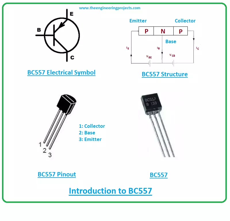
BC517 Pinout
The BC517 comes with three pins called: 1: Collector 2: Base 3: Emitter The following figure shows the pinout of BC517.
- These are also called transistor terminals that are mainly used for external connection with the electrical circuit. All these pins are different in terms of functionality and doping concentration.
- Both base and collector terminals are less doped compared to the emitter terminal. Plus, the emitter terminal carries the 100% transistor current. It is a sum of both base and collector current.
BC517 Pin Configuration
BC517 transistor comes in the following three main configurations: 1: Common emitter configuration 2: Common collector configuration 3: Common base configuration- Common emitter configuration carries the suitable voltage and current ratings required for amplification purposes. The reasons this configuration is preferred for amplification over the remaining two configurations.
- The amplification factor or current gain is an important factor of the transistor that mainly projects the capacity of any transistor it can amplify the current. It is denoted by ß.
- In BC517, the amplification factor is 30,000 which is far high than other transistors in the market. It is a ratio between output energy and input energy i.e. ratio between collector current and the base current.
- The current gain is another important factor used to describe the nature of the transistor. It is denoted by a and is known as alpha. It is a ratio between collector current and emitter current. The alpha value is always less than 1, commonly stands from 0.5 to 1.
BC517 Working Principle
- The base side is the key terminal responsible for the overall transistor action. The base terminal gets biased when a voltage is applied to this terminal.
- The base terminal acts like an electron valve that controls the number of electrons passing through the base pin. The base terminal operates similarly in the PNP transistor but here it controls the number of holes passing through it.
- During the amplification process, the small current at the base side is amplified and produced across the other terminals.

- And when BC517 acts like a switch, it converts the small current available at one side of the transistor into a larger current across the other terminals of the transistor.
- As this is an NPN transistor, here the base terminal is positive with respect to the emitter side and the emitter voltage is less positive than the collector voltage.
BC517 Power Ratings
The following table shows the absolute maximum ratings of transistor BC517.| Absolute Maximum Ratings BC517 | ||||
|---|---|---|---|---|
| No. | Rating | Symbol | Value | Unit |
| 1 | Collector-Emitter Voltage | Vce | 30 | V |
| 2 | Collector-Base Voltage | Vcb | 40 | V |
| 3 | Emitter-Base Voltage | Veb | 10 | V |
| 4 | Collector Current | Ic | 1 | A |
| 5 | Current Gain | hfe | 30,000 | |
| 6 | Power Dissipation | Pd | 625 | mW |
| 7 | Storage Temperature | Tstg | -55 to 150 | C |
- Collector-emitter and collector-base voltages are 30 & 40 respectively. While the emitter-base voltage is 10V i.e. it needs 10V to start the electron action in the transistor.
- The power dissipation is 625mW and junction temperature varies from -55C to 150C. The collector-current is 1A which means it can drive loads under 1A.
- Be careful while considering these ratings as ratings above these absolute maximum ratings can adversely affect the performance of the component. Also, don’t apply these ratings for more than the required time, else it might affect the device reliability.
BC517 Alternatives
The PNP complementary to BC517 is BC516.BC517 Applications
It is used in the following applications.- Used for amplification and switching purposes.
- Used in sensor circuits.
- Employed as an audio preamplifier and amplifier stages.
- Can drive loads under 1A.
- Used in battery chargers.
- Used in H-bridge and Astable and Bistable multivibrators.
- Used to control motor.
BC517 Physical dimensions
The following diagram shows the physical dimensions of transistor BC517. It will help you identify the space required for your electrical project.
×
![]()