


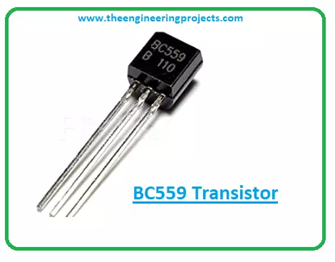
Introduction to BC559


Introduction to BC559
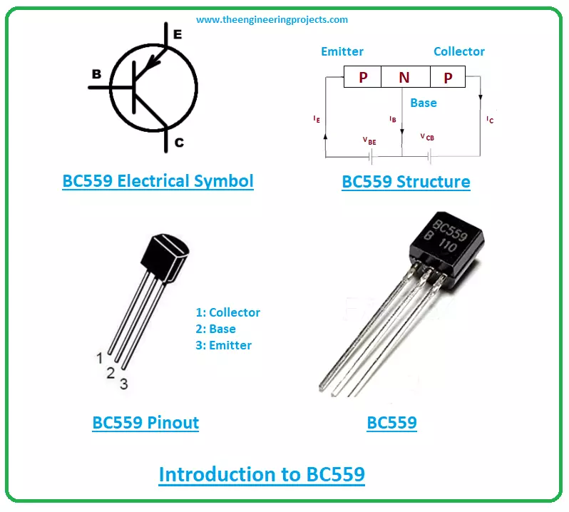
- BC559 is a PNP bipolar junction transistor mainly employed for amplification and switching applications.
- It is composed of silicon material and comes in TO-92 packaging. Based on the nature of applications and electronic projects, these transistors are also manufactured in TO-18 configuration.
- BC559 carries three terminals that are emitter, base, and collector. All these terminals are used for external connection with the circuit.
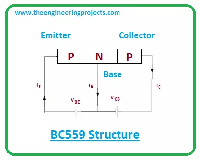
- There are three layers inside the PNP BC559 transistor where one n-doped layer stands between two p-doped layers. Here N layer represents the base terminal that is negative and the remaining two terminals are positive.
- The base terminal is still considered as the main terminal responsible for transistor action.
- Here base terminal controls the number of holes in contrast to the NPN transistor where the base is positive and controls the number of electrons.
- The emitter terminal emits the holes which are then collected by the collector terminal.
BC559 Datasheet
The datasheet gives you an overview of the main characteristics of the component. You can check the datasheet of this tiny component by clicking the link below.BC559 Pinout
BC559 is incorporated with three terminals named:- 1: Collector
- 2: Base
- 3: Emitter
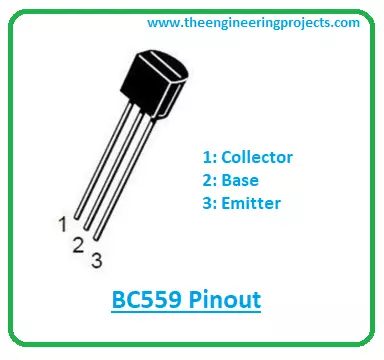
- Each terminal carries different doping concentrations and functionality as compared to the remaining two terminals. The emitter side is highly doped in contrast to the other two terminals.
BC559 Working Principle
- The working principle is simple and straight forward. When there is no current present at the base side, the transistor is turned ON and both emitter and collector are forward biased.
- And when current flows from the base terminal, the transistor is turned OFF and both emitter and collector terminals will be reverse biased.
- Though both electrons and holes contribute to conductivity, holes are major carriers in the case of this PNP transistor as opposed to NPN transistors where electrons are major carriers.
- It is important to note that NPN is preferred over PNP transistors for amplification purposes because the mobility of electrons is far better than the mobility of holes.
BC559 Power Ratings
The table given below contains the absolute maximum ratings of the BC559.| Absolute Maximum Ratings BC559 | ||||
|---|---|---|---|---|
| No. | Rating | Symbol | Value | Unit |
| 1 | Collector-Emitter Voltage | Vce | 30 | V |
| 2 | Collector-Base Voltage | Vcb | 30 | V |
| 3 | Emitter-Base Voltage | Veb | 5 | V |
| 4 | Collector Current | Ic | 100 | mA |
| 5 | Power Dissipation | Pd | 625 | mW |
| 6 | DC Current Gain | hfe | 120 to 800 | |
| 7 | Storage Temperature | Tstg | -55 to 150 | C |
- Both collector-emitter and collector-base voltage is 30V while emitter-base voltage is 5V indicating the only 5V is required to bias the transistor and start the transistor action.
- The collector current is 100mA means it can support loads under 100mA. Total device dissipation is 625mW and storage junction temperature is -55 to 155 C.
- You need to be very careful while taking these readings into consideration. If ratings exceed the desired ratings, they can terribly affect the device.
- And make sure these ratings you don’t apply for more than the required time, else they hurt the device reliability.
Difference between PNP and NPN Transistors
- Both transistors almost operate in a similar fashion i.e. base is the main terminal responsible for transistor action in both cases and emitter contains the entire current of the transistor.
- And the emitter terminal is highly doped as compared to other terminals in both cases.
- There are, however, some exceptions. The voltage polarities and current directions are reversed in both cases. Current flows from emitter to collector in case of PNP transistors while it moves from collector to emitter in case of NPN transistor.
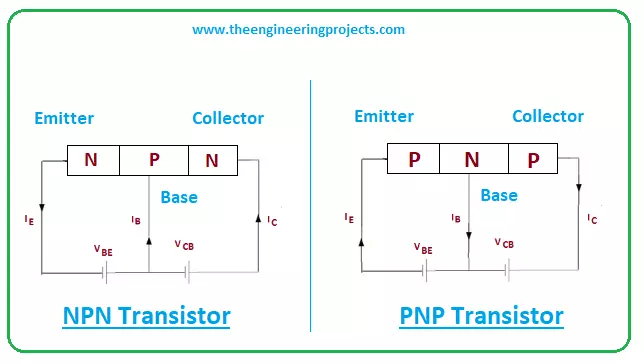
- The base terminal is negative in PNP transistor while it’s positive in the case of NPN transistor. It acts as a control valve.
- Recall NPN transistors are preferred over PNP transistors for amplification purposes because the mobility of electrons is better than the mobility of holes.
- While base terminal controls the electrons in the case of NPN transistors and it controls the holes in the case of PNP transistors.
- It is important to note that both NPN and PNP transistors are interchangeable given that if a bipolar transistor is composed of two back-to-back diodes with the base terminal being the common terminal.
BC559 Alternatives
Following transistors can be used as alternatives to BC559.- BC859 (SOT-23)
- BC858 (SOT-23)
- BC859W (SOT-323)
- BC858W (SOT-323)
- Be on the safe side and do your due diligence before starting the project.
BC559 Applications
BC559 is used in the following applications.- Finds applications in current mirror circuits.
- Used in H- Bridge circuits.
- Used for constructing Astable bistable multivibrators.
- Used to drive loads under 100mA.
- Finds application in comparator and oscillator circuits.
- Employed for switching and amplification purpose.
- Incorporated for impedance buffering.
BC559 Physical dimensions
BC559 comes in weight approx. 0.18g. The following figure represents the BC559 physical dimensions, helping you evaluate the space given for your project.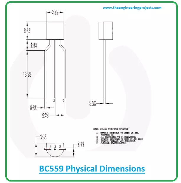
×
![]()


