


Introduction to BD140


Introduction to BD140
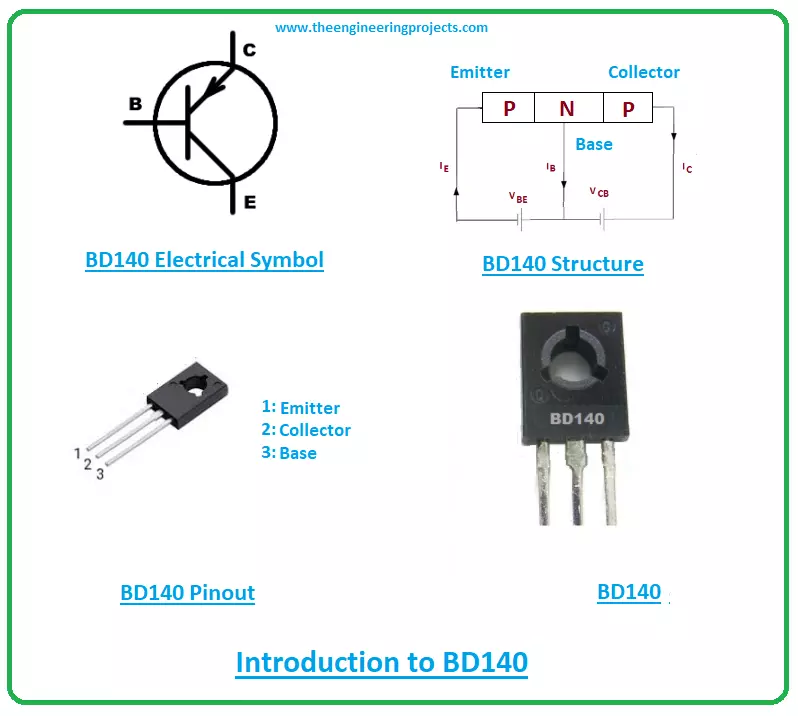
- BD140 is a PNP bipolar junction transistor that is used to drive loads under 1.5A.
- It comes with three terminals known as emitter, collector, and base. The small current at the base side is used to produce large output current at the emitter and collector terminals.
- The reason it is mainly known as a current-controlled device for controlling the input current in contrast to FETs (field-effect transistors) that are voltage-controlled devices.
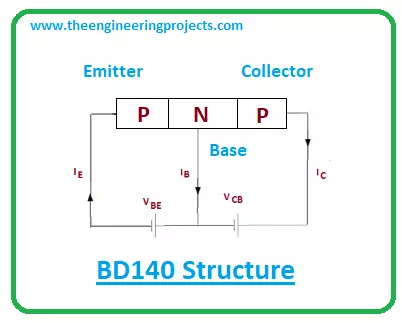
- BD140 carries three layers where one is the n-doped layer that stands between the two p-doped layers. The n-layer represents the base pin while the other two layers represent the emitter and collector terminals.
- As this a PNP transistor, here majority carriers are holes. Though both electrons and holes are necessary for the conductivity process inside the transistor, here in case of PNP transistor electrons are minority carriers and holes are majority carriers in contrast to NPN transistors where holes are minority carriers and electrons are majority carriers.
- Both NPN and PNP are termed as bipolar junction transistors and are used for amplification and switching purposes.
- NPN transistors, however, are preferred over PNP transistors for amplification purposes. Why? Because the movement of electrons inside the transistor is faster than the movement of holes in the PNP transistor.
- In rare cases, PNP and its complementary NPN are incorporated into a single electrical circuit.
BD140 Datasheet
Datasheet helps you understand the main and common characteristics of the transistor BD140. Before you install this component into your project, check the datasheet to get a hold of the main features of the transistor. Click below to download the datasheet of BD140.BD140 Pinout
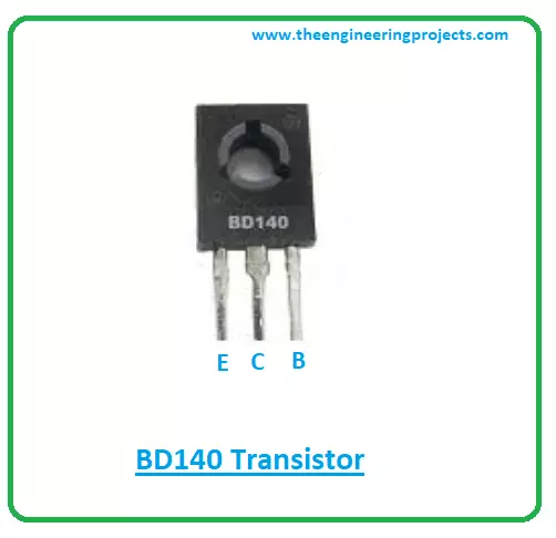
The BD140 consists of three pins named: 1: Emitter 2: Collector 3: Base The following figure shows the pinout of the BD140 transistor.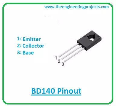
- These pins are also called terminals which are used for the external connection with the electrical circuit. All these terminals come with different functionality and different doping concentration.
- The emitter terminal is highly doped as compared to collector and base terminals. Moreover, this emitter pin consists of the entire transistor current.
BD140 Working Principle
- Whether it’s NPN or PNP transistor, the base pin is used to control the current. This base terminal controls the number of electrons in NPN transistors, and the number of holes in PNP transistors.
- In the case of this BD140 PNP transistor, when there is no current at the base side, the transistor is turned ON and both collector and emitter pins, in this case, are forward biased.
- And when there is current present at the base side, the transistor is turned OFF, leaving both collector and emitter terminals reverse biased.
Difference between NPN and PNP transistors
- Recall the base terminal is used to bias the transistor in both NPN and PNP transistors. There are, however, differ in terms of current directions and voltage polarities.
- In PNP transistor the flow of current is from emitter to collector terminal while it is opposite in NPN transistor i.e. collector to emitter terminal.
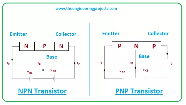
- In PNP transistor the current flows from emitter to collector terminal when a negative voltage supply is given to the base side and current flows from collector to emitter terminal in NPN transistor when positive supply is given to the base pin.
BD140 Power Ratings
The following figure shows the absolute maximum ratings of BD140.| Absolute Maximum Ratings BD140 | ||||
|---|---|---|---|---|
| No. | Rating | Symbol | Value | Unit |
| 1 | Collector-Emitter Voltage | Vce | 80 | V |
| 2 | Collector-Base Voltage | Vcb | 80 | V |
| 3 | Emitter-Base Voltage | Veb | 5 | V |
| 4 | Collector Current | Ic | 1.5 | A |
| 5 | Current Gain | hfe | 40 to 250 | |
| 6 | Power Dissipation | Ptot | 12.5 | W |
| 7 | Storage Temperature | Tstg | -55 to 150 | C |
-
- These are known as stress ratings. While working with the component, make sure ratings don’t cross the absolute maximum ratings, else they can severely damage the component and ultimately the entire project.
- The collector-emitter and collector-base voltages are 80V and only 5V are needed for the emitter-base terminals.
- This 5V voltage indicates that only 5V is required to bias the transistor and start the overall transistor action.
- The collector-current carries 1.5A which signals the amount of loads it can support.
- The power dissipation is 12.5W which illustrates the amount of energy it releases during its operation.
BD140 Alternatives
- The BD136 and BD138 are the alternatives to BD140.
- Before you incorporate these alternatives into your project, check the pinout of the alternatives. At times, the pinout of the BD140 differs from the pinout of the alternatives.
- The complementary NPN transistor to BD140 is BD139.
BD140 Applications
BD140 is used in the following applications.- Used for amplification and switching purposes.
- Used to drive loads under 1.5A.
- Used in H-bridge circuits and motor control circuits.
- Used in Astable and Bistable multivibrators.
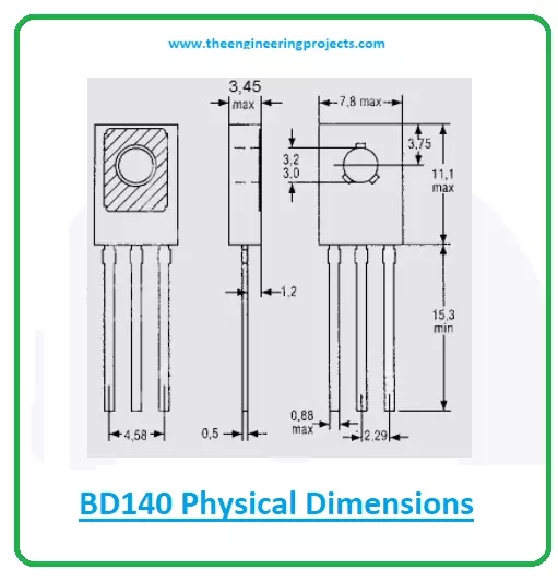
- The following figure shows the physical dimensions of transistor BD140.
- By looking at these dimensions, you can audit the total space required for the entire electrical project and you can install this component in the desired place.
×
![]()


