


CA3162 A/D Converter Datasheet, Pinout, Features & Applications


Hi Friends! I welcome you on board. Happy to see you around. In this post today, I’ll detail the Introduction to CA3162.
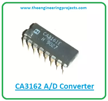
The CA3162 is a monolithic A/D converter, offering a 3-digit multiplexed BCD output. It comes with an ultra-stable internal band-gap voltage reference. With differential input, this device provides a choice of low-speed (4Hz) or high-speed (96Hz) conversion rate. It is a 16-pin device that provides dual slope A/D conversion.
I suggest you buckle up as I’ll walk you through the complete Introduction to CA3162 covering datasheet, pinout, features, and applications. Without further ado, let’s get started.
Introduction to CA3162
- The CA3162 is a monolithic A/D converter that offers a 3-digit multiplexed BCD output. It is available with ultra-stable internal bandgap voltage reference.
- To apply a complete 3-digit display, it is employed with the CA3161E BCD-to-Seven-Segment Decoder/Driver along with a minimum of external parts.
- A/D converter is a device that converts analog input signals to digital output signals.
- The environmental quantities are considered analog signals including temperature, sound, time, pressure, etc. are analog quantities.
- Analog quantities provide value at every instant of time, making it almost impossible to monitor them with digital devices.
- The reason we often have to convert analog signals to digital signals is so we can analyze this information using digital instruments like CA3162.
CA3162 Datasheet
While working with any component, it’s wise to read the datasheet of the component that details the main characteristics of the device. You can download the datasheet of this component CA3162 by clicking the link mentioned below.
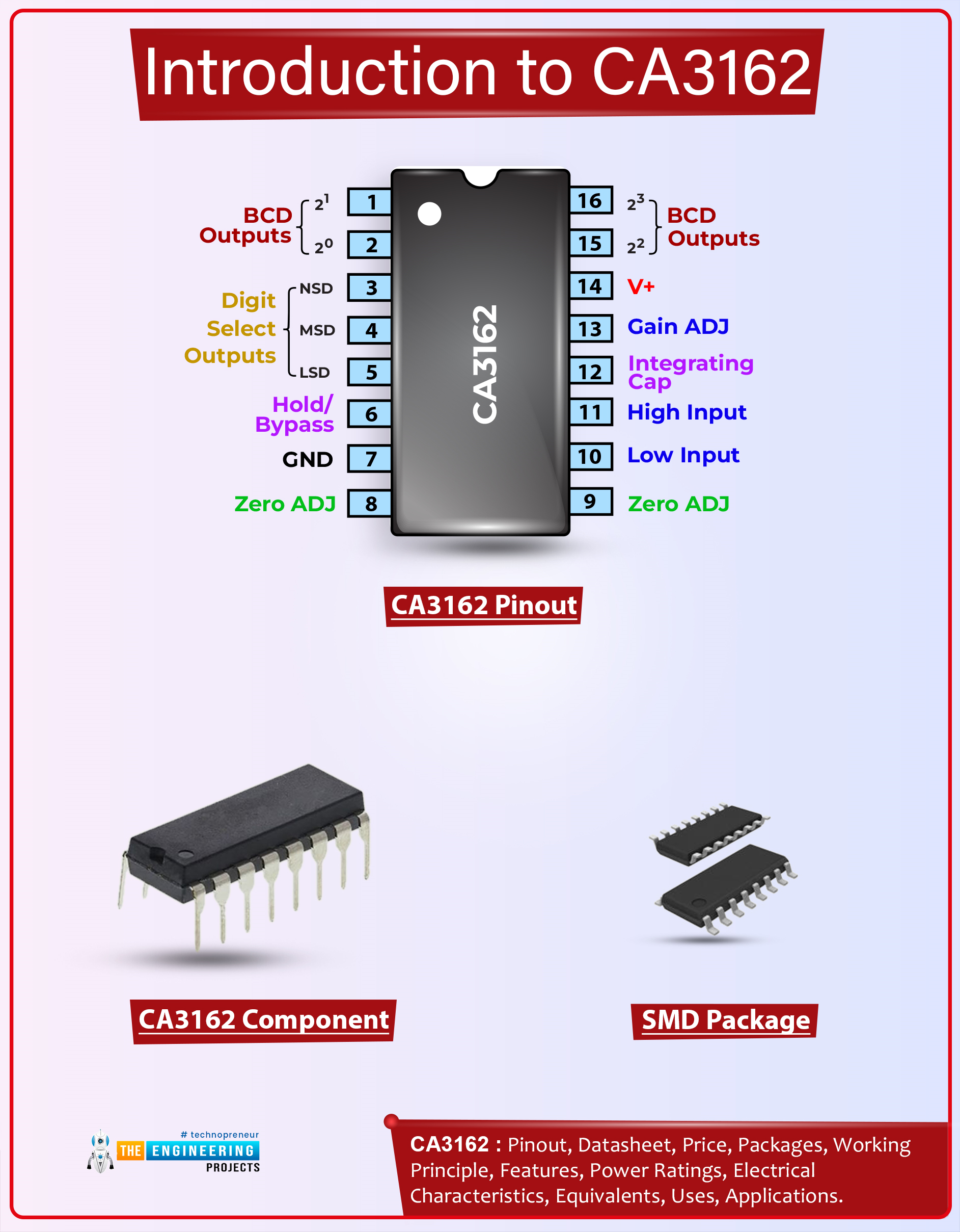
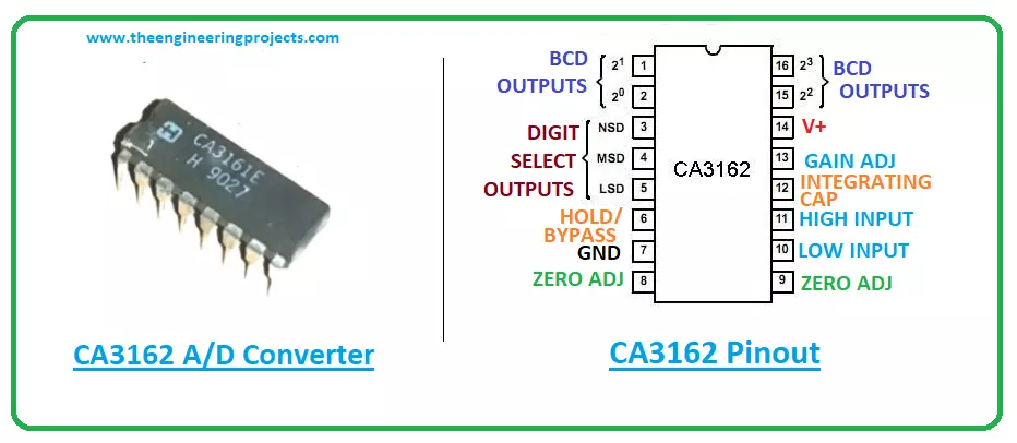
CA3162 Pinout
The CA3162 is a 16-pin device. The pinout diagram of this device is shown below.
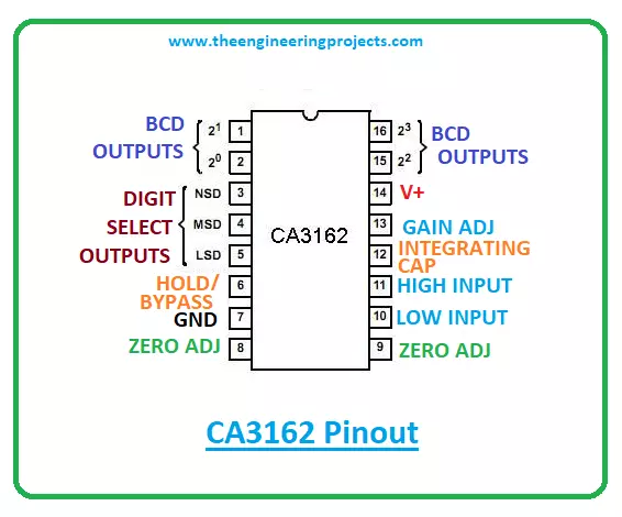
- Pin 1 & 2 are BCD outputs. Pin 3,4,5 are digit select outputs. The input at pin 6 is used to determine the sampling rate. Pin 7 is ground while Pin 8 & 9 are zero adjustment pins which are used to display the zero setting of this device.
- These pins are considered the starting point of any instrument.
- Pin 10 & 11 are low input and high input respectively which means the input voltage applied on pins 10 and 11 is converted to a current which in return charges the integrating capacitor incorporated on pin 12 for a predetermined time interval.
- Pin 14 is a voltage supply pin and pin 15 & 16 are again BCD outputs.
CA3162 Features
The following are the main features of CA3162 that help you understand how this device differs from its peers available in the market.
- Dual Slope A/D Conversion
- Multiplexed BCD Display
- Ultra Stable Internal Band Gap Voltage Reference
- Capable of Reading 99mV Below Ground with a Single Supply
- Differential Input
- Internal Timing - No External Clock Required
- Choice of Low Speed (4Hz) or High Speed (96Hz) Conversion Rate
- “Hold” Inhibits Conversion but Maintains Delay
- Internal Timing
- Overrange Indication
- “EEE” for Reading Greater than +999mV
CA3162 Applications
CA3162E can be employed in a 7-segment display or LCD.
That’s all for today. Hope you’ve enjoyed reading this post. If you’re unsure or have any questions in your mind, you can approach me in the section below, I’ll help you the best way I can. Feel free to share your valuable suggestions and feedback around the content we share, and help us create quality content customized to your exact needs and requirements. Thank you for reading the post.


