IRF3710 MOSFET Datasheet, Pinout, Features & Applications
Hello Guys! Hope you’re well today. I welcome you on board. In this post today I’ll describe the Introduction to IRF3710.
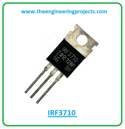
The IRF3710 is an N-channel MOSFET made up using advanced process technology. It is mainly used for fast switching purposes and comes with extremely low on-resistance. It is a fully avalanche-rated device with a gate-source voltage of around 20V.
I suggest you read this entire post till the end as I’ll detail the complete Introduction to IRF3710 covering datasheet, pinout, features, and applications. Let’s jump right in.
Introduction to IRF3710
- The IRF3710 is an N-channel MOSFET mainly employed for fast-switching purposes.
- It is manufactured using advanced process technology and comes with very low on-resistance.
- This device is composed of three terminals a drain, gate, and source. Sometimes it is also called a four-terminal device where the body is also considered as the terminal of the device.
- The electrons enter the channel through the source terminal and they exit the channel through the drain terminal. While the gate terminal is used for biasing the device.
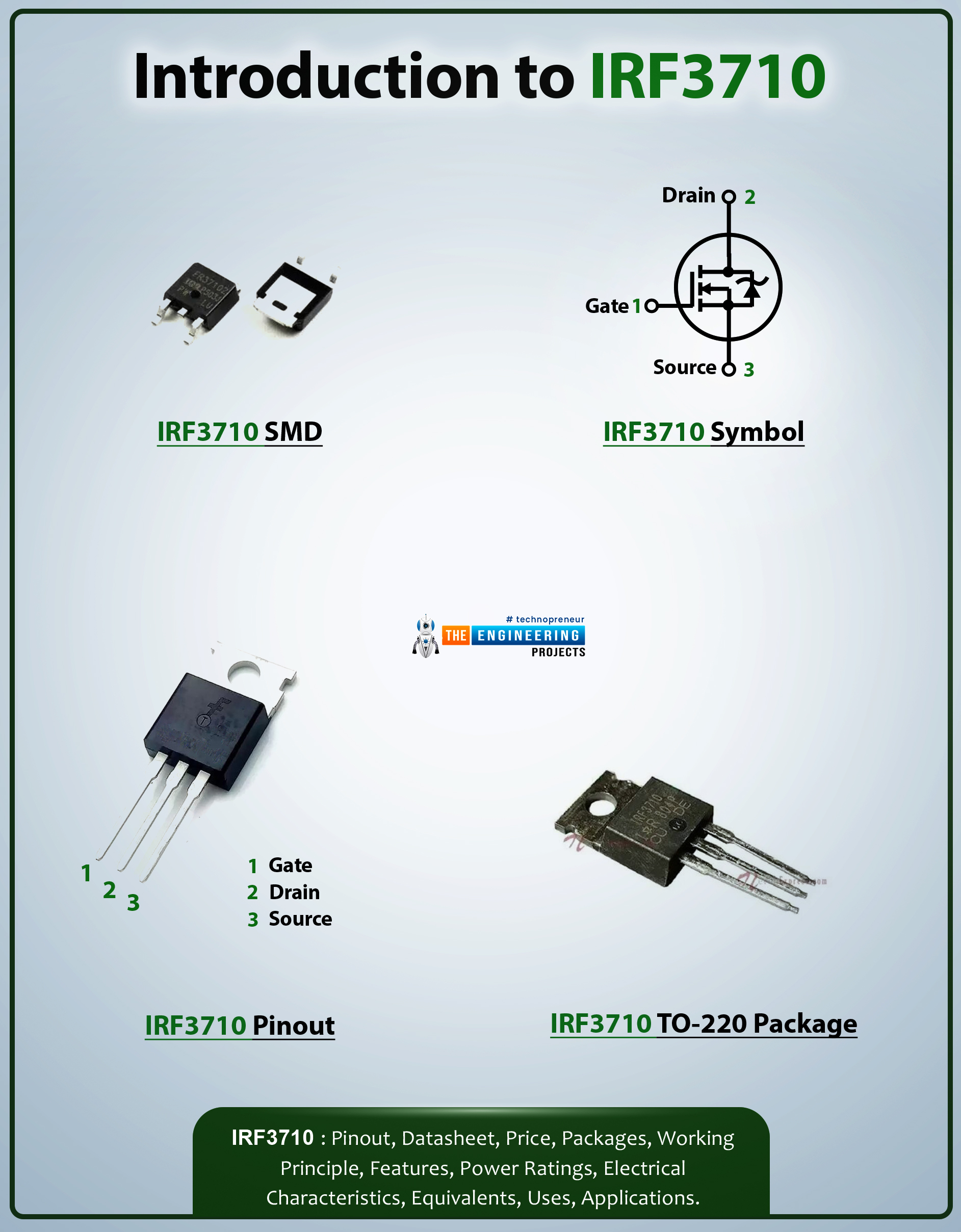
- The gate pin is located between the source and drain pin. The voltage on the gate pin is used to control the channel width.
- This IRF3710 MOSFET carries low ON resistance, making it a suitable pick for low drop switching applications. The low drop leads to low power loss, hence ensures greater efficiency.
- The MOSFETs are considered the voltage-controlled device in contrast to bipolar junction transistors that are current-controlled devices and comes with terminals base, emitter, and collector.
- The MOSFETs are mainly divided into two types i.e. N-channel MOSFET and P-channel MOSFET.
- This chip IRF3710 falls under the category of N-channel MOSFET where current is carried out by the movements of electrons as opposed to P-channel MOSFET where holes are the major charge carriers. The movement of holes is slow compared to the movement of electrons, making N-channel MOSFETs better than P-channel MOSFET for any electrical project.
- The MOSFET works in depletion mode and enhancement mode.
- During the enhancement when there is no voltage, there will be no current across the channel. While when voltage is applied across the gate terminal, it increases the conductance.
- During depletion mode, on the other hand, when no voltage is applied across the gate terminal, there is current across the channel. However, when the voltage is applied across the gate terminal, it will decrease the channel conductivity.
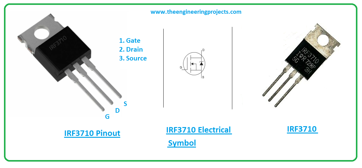
IRF3710 Datasheet
Better read the datasheet of the component before incorporating it into your electrical project. The datasheet covers the main characteristics of the device. Click the link below to download the datasheet of IRF3710.IRF3710 Pinout
The following figure shows the pinout diagram of IRF3710.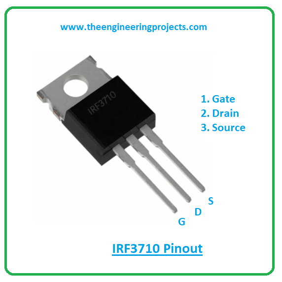
| Pin Description of IRF3710 | ||||
|---|---|---|---|---|
| Pin No. | Pin Description | Pin Name | ||
| 1 | This terminal used for biasing the device | Gate | ||
| 2 | Electrons leave the channel through this terminal | Drain | ||
| 3 | Electrons enter the channel through this terminal | Source | ||
IRF3710 Features
The following are the main features of IRF3710 MOSFET.- Type = N-Channel
- Category = IRF series
- Department = Transistors
- Drain-Source Volt (Vds) = 100V
- Advanced process technology
- Gate-Source Volt (Vgs) = 20V
- Ultra-low on-resistance
- Drain Current (Id): 57A
- Fast switching
- Power Dissipation (Ptot) = 200W
- Fully avalanche rated
- Dynamic dv/dt rating
IRF3710 Applications
The IRF3710 is used in the following applications.- Used in switching applications
- Used in USP
- Employed in Inverters
- Used in embedded projects
- Employed in instrumentation projects
That’s all for today. Hope you find this article helpful. If you have any questions, you can pop your comment in the section below. I’d love to help you the best way I can. You’re most welcome to share your valuable feedback and suggestions around the content we share. They help us create quality content customized to your exact needs and requirements. Thank you for reading the article.


