


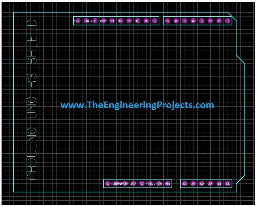
Top 10 PCB Design Software


Hello friends! Today, we will compare ten PCB design tools and learn how to choose one for an actual electronics project. A good choice should help you draw an understandable schematic, select the correct footprints, route the board and deliver files that your manufacturer can use.
There is no single program that is best for every engineer. A student building a sensor board, a developer fitting electronics inside an enclosure and a team designing a complex multilayer product have different requirements. We will compare those requirements instead of treating a longer feature list as an automatic win.
This guide updates the original collection for October 2026. Several familiar tools remain, while EAGLE's retirement and the distinction between schematic drawing and PCB layout need particular attention. The original illustrations are retained, but older interfaces should be read as historical examples rather than screenshots of current releases.
What Should PCB Design Software Do?
A PCB design begins with electrical intent. The schematic identifies components and connections; the board layout gives those connections physical copper paths. A symbol describes a component's electrical pins, while its footprint defines pads, holes and other physical features. A correct-looking symbol can still produce a faulty board if its pin numbers map to the wrong pads.
Electrical rules checking, usually called ERC, examines schematic conditions such as questionable pin connections. Design rules checking, or DRC, examines board conditions such as copper spacing and trace width. Neither checker can decide that you selected the right resistor value or chose an appropriate connector for the application.
The final workflow includes manufacturing outputs, not just a colored board image. You may need copper and solder-mask Gerbers, drill files, a board outline, a bill of materials and component placement data. Fabrication and assembly requirements differ, so establish which outputs your supplier expects before selecting a tool.
Quick Comparison of Ten PCB Design Tools
The order below is a reading order, not a measured performance ranking. Licensing and features vary by edition, so use the linked vendor documentation when checking a specific purchase. These recommendations reflect workflow suitability; they are not claims that every listed program was benchmarked on the same board.
| Tool | Useful starting point | Important selection question |
|---|---|---|
| Altium Designer | Professional boards and managed engineering workflows | Which capabilities are included in the offered solution? |
| Autodesk Fusion Electronics | Electronics and enclosure coordination | Does the selected plan fit the design and access requirements? |
| Proteus | Circuit and firmware simulation alongside board design | Are the required simulation models and layout features licensed? |
| Fritzing | Documenting simple prototypes and making small boards | Can its workflow handle the project's routing complexity? |
| DipTrace | Desktop schematic and PCB work | Do the edition's limits fit the expected board? |
| KiCad | General-purpose open-source PCB design | Can the team maintain suitable libraries and review practices? |
| DesignSpark PCB | Boards with a free entry plan and optional advanced features | Which required features belong to paid plans? |
| EasyEDA | Browser-based design and integrated sourcing workflows | Which edition and storage workflow will be used? |
| OrCAD X | PCB development with Cadence capture and analysis tools | Which package includes the needed layout and analysis functions? |
| LibrePCB | Open-source schematic and board projects | Does the current release meet the board's routing requirements? |
1. Altium Designer
Altium Designer brings schematic, layout, rules, three-dimensional inspection and manufacturing preparation into a professional design environment. Its official documentation also covers managed design data, collaboration and more specialized workflows. Availability depends on the solution and entitlement, so a feature appearing in documentation is not enough to confirm that it is included in your quotation.

I would shortlist Altium when a team needs a consistent process for reusable parts, design reviews and production releases. The benefit comes from establishing those processes, not simply installing a large application. A small one-off board may not justify the same purchasing and administration overhead.
During evaluation, build a representative circuit and create one custom component from its datasheet. Check how the schematic symbol, footprint, manufacturer information and revision history remain connected. Then generate a release package and ask the person receiving it whether the contents are complete and easy to inspect.
2. Autodesk Fusion Electronics
Fusion Electronics is the relevant Autodesk option for a new comparison. Autodesk ended EAGLE sales and support effective June 7, 2026, and its EAGLE transition notice explains the migration path. The notice distinguishes older perpetual licenses from the retired subscription and free access arrangements.

The retained image shows the earlier EAGLE environment. It is useful historical context, but it should not guide a new installation decision. Fusion combines electronics work with mechanical design, making it a candidate when board outline, connector positions and enclosure features must be coordinated.
Before migrating a project, preserve the original files and check the imported design. Inspect footprints, copper pours, design rules, text and manufacturing outputs. Compatible file formats reduce migration work, but a responsible release still requires review. Also establish how your chosen subscription handles collaboration, project access and continued use of archived designs.
3. Proteus Design Suite
Proteus is especially relevant to readers who already use our microcontroller simulations. Labcenter's PCB design overview describes schematic capture and PCB layout within the suite. Firmware simulation can complement that workflow when the necessary processor and peripheral models are available.
The practical attraction is being able to study circuit behavior and then work toward a board using familiar project data. However, a device appearing in a schematic library does not prove that it has a simulation model, a suitable footprint or a verified model of every physical characteristic.
For a sensor controller, check three separate things: the firmware can execute in the selected simulation, the electrical behavior is represented adequately, and the package matches the component you will buy. Simulation cannot certify PCB current capacity, connector strength or electromagnetic compatibility. Inspect the exact Proteus edition and purchased modules before planning the complete workflow.
4. Fritzing
Fritzing can help beginners document a breadboard prototype and understand its schematic and PCB representations. Its PCB tutorial covers arranging parts, routing and exporting manufacturing files, including Gerbers. This makes it more than a drawing tool, although its strengths differ from those of a complex professional routing environment.
I would consider it for a small educational board when visual explanation is a major part of the project. A clear breadboard illustration can help another learner understand connections. Still, the illustration and the board footprint must agree electrically; attractive artwork does not validate pad numbering.
Try a component that is not already available in a convenient library before committing to a project. Check how much effort it takes to create and review its representations. If the intended board has demanding routing, tight packaging or many constraints, evaluate those tasks directly instead of assuming that a simple first example represents the full workload.
5. DipTrace
DipTrace provides schematic-to-board conversion, component placement and routing in a desktop workflow. Its PCB layout documentation describes net classes, rule settings, interactive routing and three-dimensional preview. Check the selected edition's limits and licensing terms against the actual project.
A useful evaluation is to draw a small circuit, transfer it to the PCB and then change the schematic. Observe how the board updates and how the software reports differences. The first successful transfer is only part of a real workflow; repeated changes must remain understandable.
DipTrace belongs on a shortlist when you want an integrated desktop environment and are willing to compare its library and routing approach with alternatives. Inspect a routed board in both electrical and mechanical terms. A clean three-dimensional preview helps with component orientation and enclosure discussions, but it does not replace copper-rule checks or dimensional verification.
6. KiCad
KiCad is a strong starting point for general-purpose open-source PCB work. The KiCad PCB design overview describes interactive routing, schematic integration, custom design rules and import capabilities. Older descriptions that present it as a narrowly limited student tool no longer explain its practical range.
My recommendation for an independent learner is to evaluate KiCad early, particularly when editable local project files and an open-source toolchain matter. This is a workflow recommendation, not a promise that every advanced requirement will be effortless. Good component libraries, careful constraints and disciplined reviews still require engineering work.
Use the installed release's documentation and keep project libraries with the design when practical. A project that depends on a privately modified global footprint can become difficult to reproduce elsewhere. When importing another tool's files, inspect the translated rules and geometry before treating the imported board as an approved manufacturing source.
7. DesignSpark PCB
DesignSpark PCB offers an Explorer entry plan and paid plans with additional capabilities. The official feature comparison lists schematic and board tools, manufacturing outputs and DRC, while identifying plan-specific features such as differential-pair tools and blind or buried vias.
This makes it worth considering when a free starting workflow suits today's board and a defined upgrade path may suit later work. Read the feature matrix before designing around an advanced capability. Account requirements and software access arrangements also belong in the selection decision.
For an initial evaluation, export the copper, drill and outline files and inspect them in a separate viewer. Confirm that the dimensions and plated-hole assumptions match the order you intend to place. A convenient component catalog or quotation feature is helpful, but manufacturing data should remain understandable independently of the purchasing interface.
8. EasyEDA
EasyEDA provides browser-based electronics design and downloadable clients. Its Standard edition guide covers schematic capture, PCB layout, libraries, design-rule checking and fabrication exports. It also documents connections with component sourcing and PCB ordering workflows.
This can be convenient when you want to begin on a supported browser and move quickly between design and sourcing. Choose the edition deliberately: instructions for Standard and Professional are not automatically interchangeable, and project format or feature differences should be checked before switching.
Large public libraries are useful search resources, not a guarantee of correctness. Verify the selected manufacturer's part number, pin mapping, package dimensions and assembly availability. Keep an exported project backup and understand whether each design is private, shared or public. An ordering integration should save repetitive work while leaving you able to review the actual design.
9. OrCAD X
OrCAD X is Cadence's PCB development platform, with schematic, layout and analysis capabilities offered through different packages. The OrCAD X product FAQ explains the tiers and requirements. PSpice is a circuit-simulation tool within this broader ecosystem, so the two names should not be used as synonyms.
I would evaluate OrCAD X when the existing team, customers or design data already use Cadence workflows, or when the required analysis tools justify the environment. Ask for a demonstration using your own kind of circuit rather than only a prepared marketing example.
During the trial, check how constraints move from schematic intent to physical layout and how reviewers inspect them. Confirm which analysis and collaboration features are included. Training, compatible project access and the ability to reproduce a released design are part of the cost, alongside the software license itself.
10. LibrePCB
LibrePCB is another open-source option to investigate. Its project feature overview introduces the cross-platform approach and links to its schematic editor, board editor, libraries and output tools. It offers a different design and library workflow from KiCad, so choosing between them should involve a small practical exercise.
Evaluate how a component is represented, assigned to a package and reused across designs. Then test the routing and output operations your board actually requires. Do not infer support for a specialized high-speed feature merely because a program can create a multilayer PCB.
For a modest controller or educational board, an understandable workflow can be more valuable than an unused collection of advanced commands. Record the application version and preserve the complete project. Open-source availability helps long-term access, but it does not remove the need to keep libraries and design decisions with the files.
What About TinyCAD, ZenitPCB and ExpressPCB?
The original article also included TinyCAD, ZenitPCB and ExpressPCB. TinyCAD deserves a specific correction: it is a schematic tool that can export connectivity to another PCB application. Its netlist documentation explains this handoff; it does not make TinyCAD a complete board-placement and routing environment.
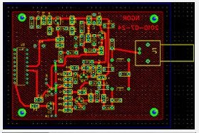
The TinyCAD illustration is retained for that schematic role. Existing ZenitPCB and ExpressPCB projects should be evaluated according to the version, available support and manufacturing workflow they actually use. This updated shortlist is not a reason to abandon a working archived design, but a new project needs a confirmed installation and output path.
How to Compare Tools Using One Small Board
- Choose a representative low-voltage circuit with a power connector, regulator, microcontroller or sensor, decoupling capacitors and test points.
- Create one custom symbol and footprint from a real datasheet.
- Define the board outline and mounting holes before routing.
- Enter manufacturing rules supplied by the intended fabricator.
- Place critical components and route the board manually enough to understand the return paths.
- Make a schematic change and update the layout.
- Run checks, export the manufacturing files and inspect those files independently.
Record where you needed help, which operations were unclear and whether another person could reopen the project. This comparison measures the tasks you will repeat. Timing how quickly an autorouter finishes an unfamiliar example tells you much less about the complete engineering process.
Use calculations to guide the layout
Even a simple trace has resistance. A first approximation is R = ρL/(wt), where ρ is copper resistivity, L is length, w is width and t is copper thickness. Using approximately 1.72 × 10⁻⁸ Ω·m for copper near 20°C, a 50 mm trace that is 0.5 mm wide and 35 micrometres thick has roughly 0.049 Ω resistance. Texas Instruments discusses the material and temperature assumptions in its copper PCB resistance design note.
At 1 A, that approximation gives a 49 mV drop and 49 mW of dissipation through P = I2R. It is a resistance estimate, not a current-rating rule. Temperature rise depends on the board construction and surroundings, while vias and connectors add resistance. Use the example to see why a thin signal trace and a power path may need different constraints.
Units also cause practical mistakes: one mil is 0.001 inch, or 0.0254 mm. A 10 mil trace is 0.254 mm wide. Confirm which units the rule editor expects and avoid copying a spacing value without its unit. A perfectly enforced rule is still wrong if it describes the wrong manufacturing process.
Review the Design Before Ordering
Check footprints against package drawings, including pin one, connector orientation, hole sizes and mechanical clearance. Read the bill of materials against the actual schematic. Resolve every unexplained DRC issue and document deliberate exceptions. Unconnected pads, overlapping copper and incorrect net assignments require different explanations.
Inspect exported files rather than relying only on the editor. Confirm that the board outline is closed, the drill file is included, copper layers are correctly identified and silkscreen does not hide assembly information. Preserve the exact release package so that later orders can be tied to the same revision.
Frequently Asked Questions
Which tool should a beginner try first?
KiCad is a sensible general-purpose starting point; Fritzing may suit a small project centered on visual prototype documentation. If your course uses Proteus or another specific tool, following that environment can reduce unrelated setup work while learning the electrical fundamentals.
Do I need the most expensive software for a reliable PCB?
No. Reliability depends on the circuit, layout, component choices, manufacturing requirements and review process. Advanced software can help manage difficult requirements, but it cannot supply missing engineering assumptions automatically.
Can simulation replace a prototype?
Simulation helps investigate modeled behavior. A physical prototype reveals assembly, loading, noise, thermal and mechanical effects that may not be represented. Use both according to the questions you need to answer.
Is an autorouted board ready for manufacture?
No. Routing completion only means connections were attempted under the configured rules. Review return paths, power distribution, sensitive signals, thermal behavior and manufacturing outputs before release.
Should I change software in the middle of a working project?
Only when there is a clear benefit or requirement. Preserve the original, trial the migration on a copy and compare outputs before replacing the established workflow. A familiar, supported process is often more useful than switching tools without a defined reason.

Comments
0