Introduction to ATmega4809


Introduction to ATmega4809
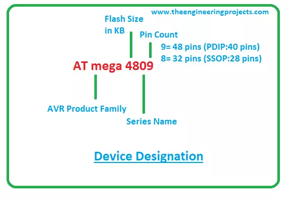
- The ATmega4809 microcontroller belongs to the megaAVR® 0-series that contains an AVR processor.
- The series carries low power features with the latest core independent peripherals.
- The ATmega4809 utilizes Microchip's latest technologies with an efficient and low-power architecture including SleepWalking, Event System, and accurate analog features.
- This device carries Single-pin Unified Program Debug Interface (UPDI) that is a bi-directional single wire interface and needs a programmer that supports UPDI.
- The clock speed is 20MHz which is required for the synchronization of all internal functions.
- The microcontroller program is stored in the flash memory which is around 48KB. While EEPROM and SRAM are 256bytes and 6KB respectively. Write/Erase endurance for flash memory is 10,000 cycles and for EEPROM is 100,000 cycles.
- SRAM memory is used to produce and manipulate variables when this runs. The EEPROM memory is a non-volatile memory that stays stored in the board even when board power is removed.
- There are 4 UART communication protocols and one SPI and one I2C communication protocol are available on the microcontroller.
- The UART is a serial communication protocol that carries two pins Rx and Tx. The Rx is a receiving pin that is used to receive the serial data while Tx is a transmission pin used to transfer serial data.
- I2C is a two-wire communication protocol that carries two pins SDL and SCL. The SDL is a serial data line that carries the data while SCL is a serial clock line that is used for the synchronization of all data transfer over an I2C bus.
- SPI stands for a serial peripheral interface that is mainly used to develop the communication between the controller and other sensors and shift registers. Two pins: MISO (Master Input Slave Output) and MOSI (Master Output Slave Input) are incorporated for SPI communication. These pins are installed to receive or send data by the controller.
- This device comes with three sleep modes: Idle, standby, and power down. The sleep mode is the mode when nothing happens. Simply put, during sleep mode device remains in rest mode. As nothing taking place during the sleep mode, at that point the device consumes the lowest power and the crystal oscillator is turned off.
- The device also offers a power-on-reset (POR) and brown-out-detection (BOD). The power-on-reset just resets the device when the signal is provided to the device.
- The brown-out-detection is a protection circuit that monitors when the supply voltage goes below down a certain level and consequently puts the device into a reset state which leads to proper startup when power is applied back again.
- The controller also contains 16-channel 10-bit ADC and an analog comparator.
- Other features include configurable custom logic, 5x16 bit timer, cyclical redundancy check, watchdog timer, and hardware multiplier.
ATmega4809 Datasheet
Before you incorporate this device into your electrical project, it’s wise to scan through the datasheet of the component that features the main characteristics of the device. Click the link below and download the datasheet of ATmega4809.Available Packages
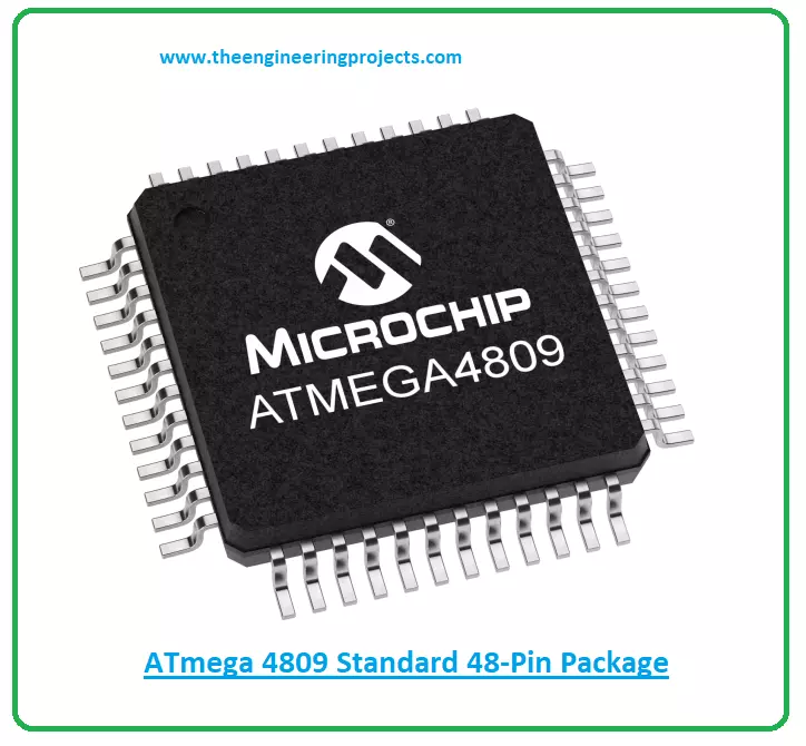
ATmega4809 comes in different pin mappings mainly dependent on the current hardware.48 Pin Package
It is the standard pin package that comes with 9 PWM pins and a flash memory of 48KB. Know that this 48-pin package is only available on ATmega4809 and ATmega3209.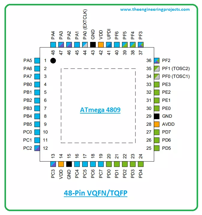
40 Pin Package
This pinout is almost identical to the 48-pin package with lesser pins and it comes with 8 PWM pins.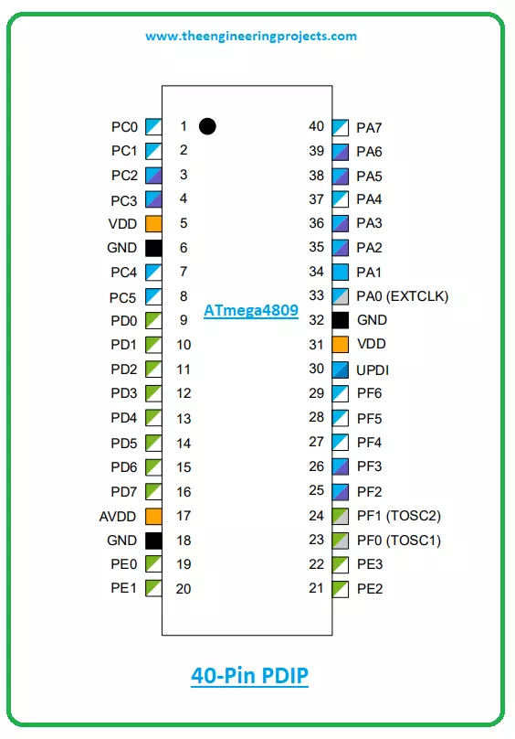
32-Pin Package
This pinout is a robust and clean design that comes with 8 PWM pins.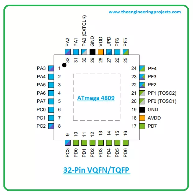
28-Pin Package
This is the 28-pin package that comes with 8 PWM pins and a clock frequency of around 20MHz. Again, this pinout is also not compatible with Arduino shields.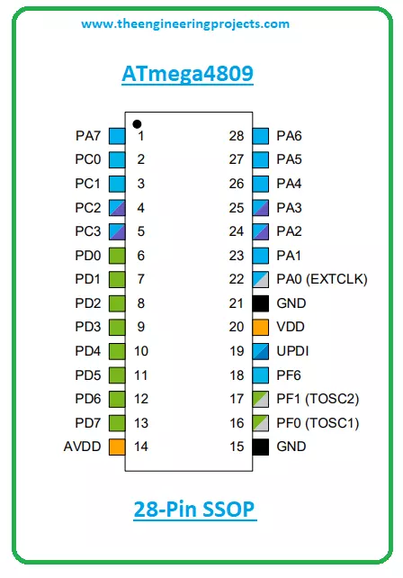
Uno WiFi
The Arduino Uno WiFi Rev2 hardware incorporates this pinout. It comes with 6 PWM pins. Any code written for Arduino UNO WiFi Rev 2 is equally compatible with this pinout. It is important to note that Uno WiFi pinout is only reserved for ATmega3209/4809.Nano Every
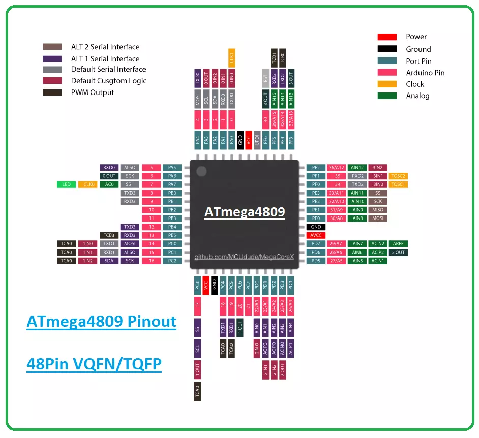
The Arduino Nano Every incorporates this pinout. The code written for Arduino Nano Every can run for this pinout without any modifications. You’ll get this pinout when you select ATmega4809 from the Arduino IDE software.ATmega4809 Pinout
The following figure shows the pinout diagram of ATmega4809 that comes in a 48-pin package.
ATmega4809 Features
- No. of pins = 48
- Flash memory = 48KB
- SRAM = 6KB
- EEPROM = 256 bytes
- Also includes Hardware multiplier
- Three sleep modes: Idle, Standby, Power Down
- Event System for core independent and predictable inter-peripheral signaling
- Comes with Power-On Reset (POR) and Brown-Out Detection (BOD)
- Contains Single pin programming and debugging interface (UPDI)
- Carries 16 Channel 10-bit ADC with Voltage Reference
- Features Analog Comparator (AC) and Watchdog Timer
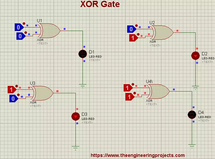
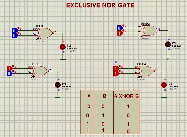
- Configurable Custom Logic (CCL) with up to four programmable Look-up Tables (LUT)
- Contains 5x 16-bit Timer (TCA / TCB) and Cyclical Redundancy Check (CRC/SCAN)
- SPI / I2C / USART
- Five selectable internal voltage references: 0.55V, 1.1V, 1.5V, 2.5V, and 4.3V
ATmega4809 Applications
- Employed in high responsive command and control applications.
- Used in embedded systems and real-time control systems.
- Used in industrial automation and home automation.
×
![]()