Hello friends, I hope you are doing well. This is the tenth tutorial in our series on how to create a Proteus library. In the previous tutorial, How to Create Your Own Library File in Proteus, we created our own library TEPTUTORIAL with the Library Manager and moved our Traffic Light Module into it. The part can be picked, placed and wired, but it has no PCB footprint yet, so it cannot be placed on a circuit board. Today, we change that. Our topic is how to create a PCB footprint and package in Proteus.
We will see what a footprint and a packaging are, look for a suitable footprint among the thousands that come with Proteus, draw our own footprint in PCB Layout with pads, a silkscreen outline, a pin 1 mark and our TEP label, store it with Make Package, link it to our part with the Visual Packaging Tool and check the result on a board and in Pick Devices.
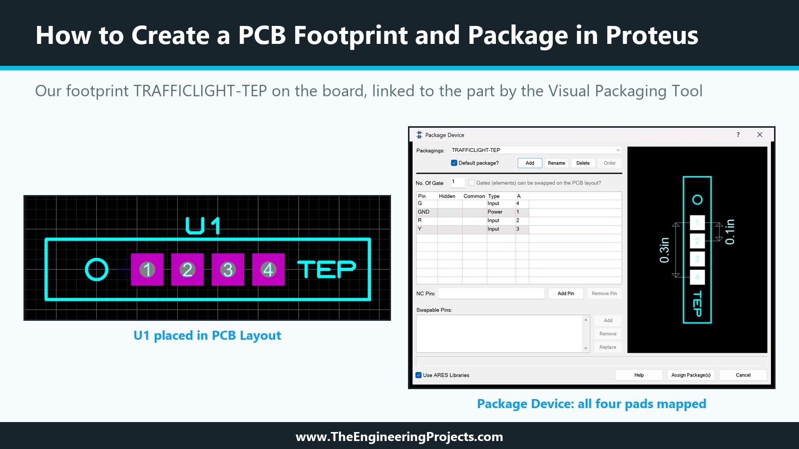
Everything in this tutorial was done in Proteus 8.5 Professional on our PC, in the same Traffic Light Module project. The picture below shows the result: our own footprint TRAFFICLIGHT-TEP placed on the board as U1, and the Visual Packaging Tool with all four pins of the part mapped to its pads.
Footprint, Package and Packaging: What Is the Difference?
Three words describe the PCB side of a part in Proteus, and it helps to keep them apart from the start.
- Footprint or package. The help defines a package as a collection of pads and silkscreen graphics used to site a component on the board. Other programs call it a footprint; Proteus stores it in a package library, and we use both words for the same thing.
- Packaging. The link from a device to a package, together with the map from the device's pins to the package's pads. One device can carry several packagings, for example a through-hole and a surface mount version of the same chip.
- PACKAGE property. The property of a component that names the package to use on the board. The help notes that most supplied parts have it embedded, which is why they appear on a board with the right footprint.
Package libraries are separate from device libraries. Proteus comes with libraries such as PACKAGE and CONNECTORS, all read-only, and with USERPKG, the read/write package library for your own footprints. A device in TEPTUTORIAL can use a package from any package library; the device only stores the package's name and the pin map.
Why Our Part Needs a Footprint
As we saw in the seventh tutorial, a part used only for simulation can do without a package. Our Traffic Light Module will mainly be simulated, but a real module is also plugged into real boards, through a four-pin male header with 0.1 inch (100 thou, 2.54 mm) spacing. If a student designs a shield or a carrier board for it, the part needs a footprint with four holes at exactly that spacing.
One detail must not be copied from the schematic: our schematic pins are 200 thou apart, a choice we made in the second tutorial for readable labels. The schematic is a drawing; the footprint is a physical layout. Its pads must match the real header, so they are 100 thou apart.
How to Draw a PCB Footprint in Proteus: Step by Step
The footprint takes five steps: check what Proteus already has, set up PCB Layout, place the pads, draw the silkscreen and store the result with Make Package.
Step 1: Look for an Existing Footprint
Before drawing anything, check whether Proteus already has a footprint that fits. In PCB Layout, select the Package mode, click the P button above the object selector and type a keyword. For "SIL", the Pick Packages browser found 50 packages, among them CONN-SIL4, a "4 way SIL header, 100th pitch" from the CONNECTORS library, with the category Connectors, the type Through Hole and the sub-category SIL Headers. Its preview shows four pads, 0.1 inch apart and 0.3 inch from the first to the last.
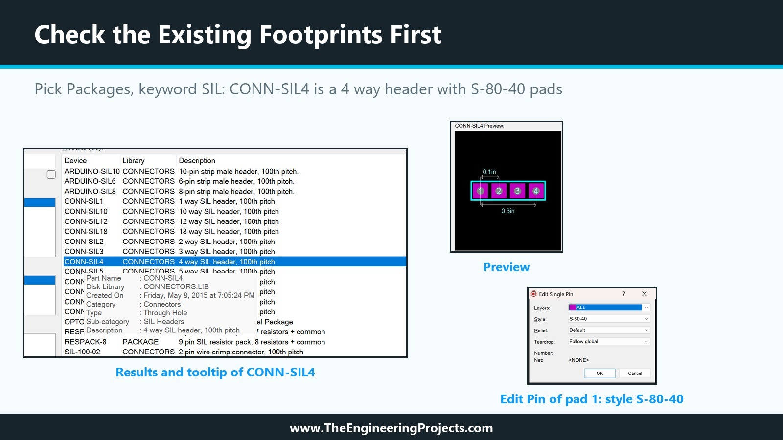
CONN-SIL4 would fit our module electrically. We placed it for a moment on an empty board, right-clicked its first pad and chose Edit Pin, which showed the pad style S-80-40 on ALL layers, meaning all copper layers. All four pads of CONN-SIL4 use this square style. We will use the same style for our own footprint, because Labcenter's own header footprint uses it for exactly the same kind of pin. The name suggests an 80 thou square pad with a 40 thou hole; you can check the exact values of any pad style before relying on them.
So why draw our own? A footprint of our own can show more than the header: our outline marks the 800 thou width of the module, so nothing tall is placed where the module stands, and our label TEP identifies the part on the board. It is also the best way to learn how footprints are made, which you will need for any module that Proteus does not have.
Step 2: Open PCB Layout and Set the Snap
PCB Layout opens from the toolbar of the project, like Schematic Capture, as a new tab. We drew our footprint on the empty board of our project and removed the drawing again after storing it, so the board is not affected.
The snap settings of PCB Layout differ from those of the schematic editor. The View menu offers Snap 1th (Ctrl+F1), Snap 5th (F2), Snap 25th (F3) and Snap 50th (F4), and Snap 25th was selected when we opened the layout. The coordinates appear at the bottom right of the window in thou, with the origin marked by a blue cross. Goto Position (Ctrl+G) moves the pointer to typed coordinates, which is useful for footprints with odd dimensions.
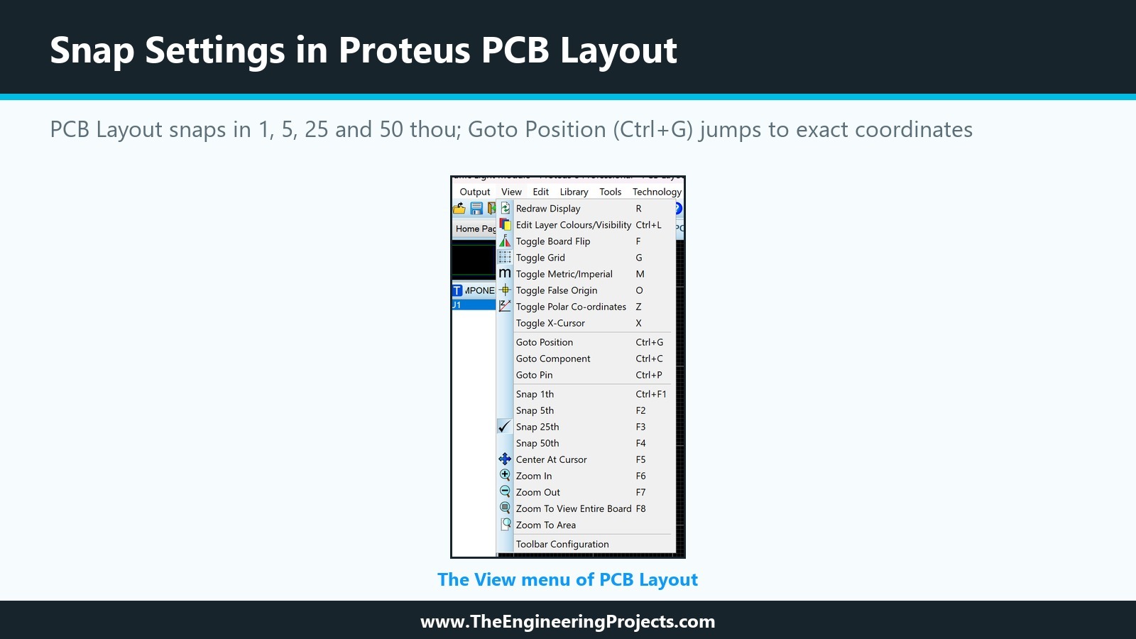
We used Snap 50th for the pads, because 100 thou is a multiple of 50, and Snap 25th for the outline. Before every click, we checked the coordinates at the bottom right; at our zoom level, 100 thou was about 57 pixels on the screen, and guessing from the grid alone put two of our first pads 50 thou off. We undid them with Ctrl+Z and placed them again after reading the coordinates.
Step 3: Place the Pads in Order
Select the Square Through-hole Pad mode in the toolbar on the left. The object selector lists the square pad styles, from DILSQ and S-40-15 up to S-150-65; we chose S-80-40. The layer selector at the bottom left shows ALL, which places through-hole pads on all copper layers, as the help recommends for through-hole parts.
Then place the pads, one click each. We placed pad 1 at the origin, (0, 0), and pads 2, 3 and 4 at 100, 200 and 300 thou on the same line. The order matters: the help explains that PCB Layout numbers the pads from 1 upwards in the order they are placed, unless you renumber them with the Auto Name Generator on the Tools menu or edit them one by one. Placing them from left to right in the order of the real header, GND, R, Y, G, gives exactly the numbers our pins already carry.
Two Practical Lessons
Two practical lessons from our PC. First, the first click after selecting a tool sometimes only activates the board and places nothing, so look before you click again. Second, while a placement tool is armed, a click outside the board area, even on the toolbar or a menu, can place a pad at the edge of the board. End the tool with a right-click on an empty part of the board before you use the menus.
Step 4: Draw the Silkscreen Outline, Pin 1 Mark and Label
Silkscreen graphics are drawn with the 2D graphics tools, like in the schematic editor, but on a board layer. Select the 2D Graphics Box tool and set the layer selector to Top Silk. We drew the outline from (-250, 75) to (550, -75): 800 thou wide, centred on the four pads, and 150 thou high, which leaves room around the 80 thou pads, because silkscreen on a pad would print onto the solder area.
Next to pad 1, we drew a small circle with the 2D Graphics Circle tool, centred at (-125, 0) with a radius of 25 thou: the pin 1 mark that every builder looks for. Finally, the 2D Graphics Text tool placed our label TEP at the right end of the outline, centred, 60 thou high and 50 thou wide, in the free space beside pad 4.
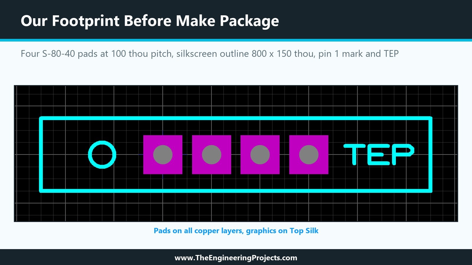
We did not place an Origin marker. The help explains that without one, the reference point of a package is the centre of the first pin placed, which is our pad 1. You can also place REFERENCE and VALUE markers to fix where the part's labels appear on the board; without them, PCB Layout chooses a position, and we kept that default.
Step 5: Store the Footprint with Make Package
Tag all objects of the footprint. Our board held nothing else, so we right-clicked an empty spot and chose Select All Objects; on a busy board, drag a tag box around the footprint instead. Then choose Make Package from the Library menu of PCB Layout.
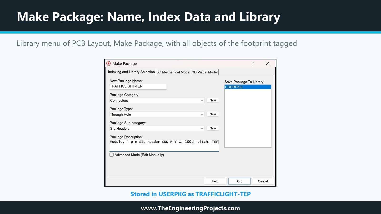
The Make Package dialogue has three tabs: Indexing and Library Selection, 3D Mechanical Model and 3D Visual Model. On the first tab we entered:
- New Package Name: TRAFFICLIGHT-TEP, ending in TEP like our device name.
- Package Category: Connectors, chosen from the list, which offered Connectors, Discrete Components, Integrated Circuits and Miscellaneous. The help states that a category is mandatory, because it indexes the package for the browser.
- Package Type: Through Hole; the other choices were Surface Mount and Surface Mount (IPC7351).
- Package Sub-category: SIL Headers, the same as CONN-SIL4.
- Package Description: "Traffic Light LED Module, 4 pin SIL header GND R Y G, 100th pitch, TEP", with the words people will search for.
- Save Package To Library: USERPKG, the only writable package library on our PC; the help notes that only libraries with write access appear here.
We left the 3D tabs empty; a 3D model only matters for the 3D viewer, and the help describes how to add one later. After OK, the package appeared in the package list of the object selector, and USERPKG.LIB had grown from 8,032 to 8,739 bytes. We then deleted the drawing from the board, because the footprint now lives in the library.
How to Link the Footprint to Your Part
With the footprint in USERPKG, three more steps link it to our part, store the part again and test the result.
Step 6: Link the Footprint with the Visual Packaging Tool
Back in Schematic Capture, we right-clicked U1 and chose Make Device, as in the eighth tutorial. On the Packagings page, which still said that no packagings were defined, Add/Edit opened the Package Device dialogue, the Visual Packaging Tool. It already listed our four pins with their types and numbers: G Input 4, GND Power 1, R Input 2 and Y Input 3.
The Add button opened the Pick Packages browser, where the keyword TRAFFICLIGHT found our new package in USERPKG at once, with the dimensions 0.1 inch and 0.3 inch in its preview. After OK, the Visual Packaging Tool showed TRAFFICLIGHT-TEP as the packaging, with Default package ticked, and all four pads in its preview turned white.
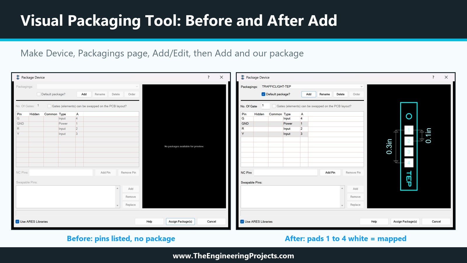
White pads are the tool's way of saying that a pin is mapped onto the pad. Ours mapped themselves: the help explains that a pad maps onto the pin with the same number when the pins have default pin numbers, and we gave GND 1, R 2, Y 3 and G 4 in the sixth tutorial. If you leave the pin numbers empty, you type them into the grid, or click a pin's field and then the pad in the preview, and the tool moves on to the next pin.
More Options of the Visual Packaging Tool
The tool has more options for bigger parts, all described in its help page:
- No. of Gates sets the number of elements for multi-element parts such as a quad NAND gate; ours is a single element.
- NC Pins records pads that are not connected, so that the preview shows every pad as accounted for.
- Add Pin creates a hidden pin that exists only in this package, typically a power pin that is connected by its name.
- Swappable Pins defines groups of electrically identical pins that may be swapped on the board.
- Use ARES Libraries validates the package against the PCB libraries; only untick it when the schematic goes to another PCB program.
Assign Package(s) closed the tool, and the Packagings page now listed TRAFFICLIGHT-TEP with its preview.
Step 7: Check the PACKAGE Property and Store the Part
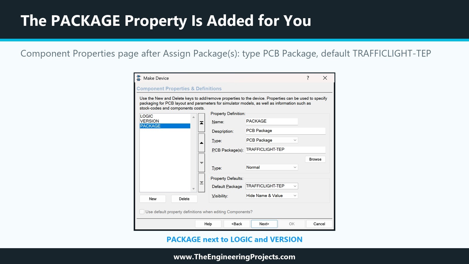
On the Component Properties page, a third property had appeared below LOGIC and VERSION: PACKAGE, with the description PCB Package, the type PCB Package, the package list TRAFFICLIGHT-TEP, Normal, and the default package TRAFFICLIGHT-TEP, hidden on the schematic. We did not have to add it ourselves.
On the Indexing and Library Selection page, one thing needs attention: the Save Device To Library list was set to 74CBT, the first writable library in the list, not to TEPTUTORIAL. We scrolled down and selected TEPTUTORIAL before clicking OK. Then Proteus asked the two familiar questions from the eighth tutorial: the device already exists in the disk library, replace it? Yes. Update all instances on the schematic? OK. TEPTUTORIAL.LIB grew from 9,836 to 13,792 bytes.
The script stored in the library now carries the package. We read it from the library file:
{*DEVICE}
{PREFIX=U}
{NOTES=Made in the TEP tutorial series How to Create a Proteus Library. Simulation model follows later in the series.}
{*PROPDEFS}
{LOGIC="Lamps light when the pin is",HILOW}
{VERSION="Library version",READONLY STRING}
{PACKAGE="PCB Package",PACKAGE,1,TRAFFICLIGHT-TEP}
{*INDEX}
{CAT=Optoelectronics}
{SUBCAT=LEDs}
{MFR=The Engineering Projects}
{DESC=Traffic Light LED Module - red, yellow and green lamps, pins GND R Y G, pin HIGH lights the lamp}
{*COMPONENT}
{LOGIC=1}
{VERSION=1.0}
{PACKAGE=TRAFFICLIGHT-TEP}
*PINOUT TRAFFICLIGHT-TEP
{ELEMENTS=1}
{PIN "G" = 4}
{PIN "GND" = 1}
{PIN "R" = 2}
{PIN "Y" = 3}
Compared with the script of the eighth tutorial, three things are new: the definition of PACKAGE in {*PROPDEFS}, with its type and the list of allowed packages; the default PACKAGE=TRAFFICLIGHT-TEP in {*COMPONENT}; and the *PINOUT section for the package TRAFFICLIGHT-TEP, which maps each pin name to a pad number. The pinout is the packaging in plain text: one element, pin GND on pad 1, R on pad 2, Y on pad 3 and G on pad 4.
Step 8: Test the Footprint on a Board and in Pick Devices
In PCB Layout, Component mode now listed U1 in the object selector, with our footprint as its preview. We placed it on the board: the four pads appeared numbered 1 to 4, with the outline, the pin 1 mark, TEP and the reference U1 above it, as in the picture at the top of this tutorial.
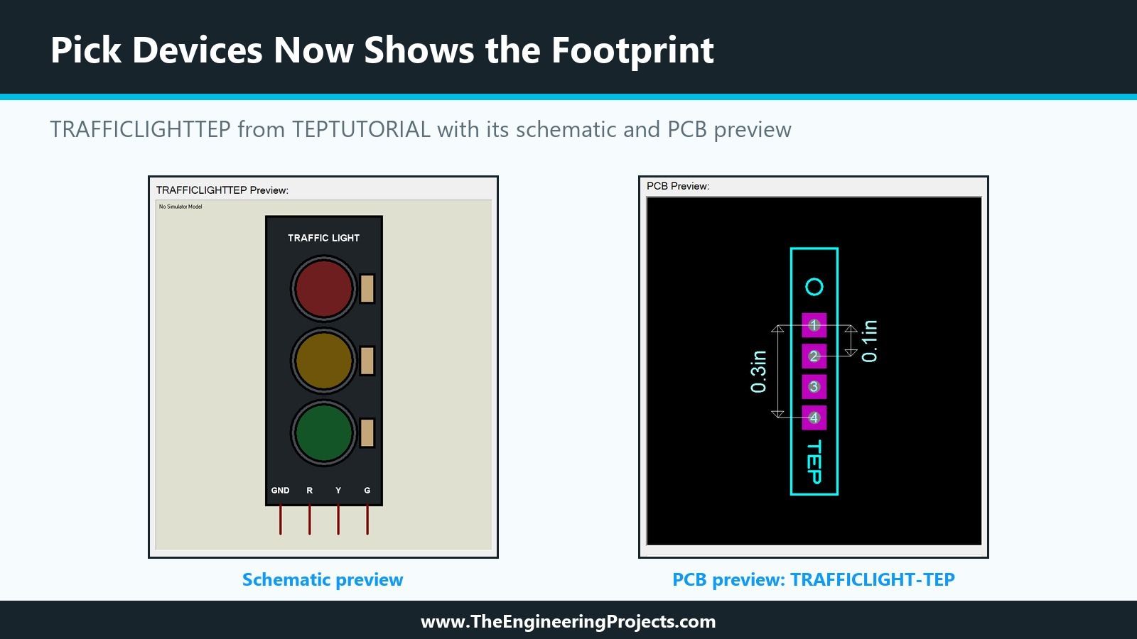
In Pick Devices, the keyword "traffic" found TRAFFICLIGHTTEP in TEPTUTORIAL with its new creation time, and the PCB Preview, which said "no PCB package" in the seventh tutorial, now shows TRAFFICLIGHT-TEP. Unlike the move with the Library Manager in the previous tutorial, this change appeared in Pick Devices without a restart.
For larger designs, the help describes two more checks. The Design Explorer lists the package of every component and marks parts without one as MISSING; and Verify Packagings on the Library menu checks that every package exists in the PCB libraries and that every pin number exists in its package.
Where the Footprint Lives and How to Share It
Our device is in TEPTUTORIAL, but its footprint is in USERPKG.LIB, a different library file. That matters when the library is shared: whoever installs TEPTUTORIAL also needs the footprint, otherwise the part has a PACKAGE property that names a package they do not have. For now, USERPKG keeps the footprint safe on our PC; in the last tutorial of the series, when we package everything for sharing, we will move the footprint into a package library of its own with the Library Manager, the same way we moved the device in the previous tutorial.
Common Mistakes When Creating a Footprint in Proteus
| Problem | Cause | Solution |
|---|---|---|
| Pads are numbered in the wrong order | They were placed in a different order | Place them in pin order, or renumber with the Auto Name Generator |
| Pads are not on the intended pitch | Placed by eye from the grid | Read the coordinates before each click, or use Goto Position |
| Pads appear on one copper layer only | The layer selector was not on ALL | Select ALL for through-hole pads |
| The outline prints over the pads | Silkscreen drawn across the pad area | Keep the outline clear of the pads |
| Extra pads appear at the edge of the board | Toolbar or menu clicked while a pad tool was armed | End the tool with a right-click on empty board first |
| Pads stay dark in the Visual Packaging Tool | Pin numbers do not match pad numbers | Type the pad numbers in the pin grid |
| The part is stored in the wrong library | Save Device To Library still on the first entry | Select your own library on the last page of Make Device |
In the Next Tutorial
Our Traffic Light Module now has a footprint as well as its graphics, pins and properties. In the next tutorial, How to Edit and Update an Existing Component in Proteus, we will change the part after it is in use: decompose it, edit its graphics and pins, store it again and see how Proteus updates the designs that already contain it.
FAQ
How do I create a new footprint in Proteus?
In PCB Layout, place the pads with a pad tool in the order of the pin numbers, draw the outline on Top Silk with the 2D graphics tools, tag everything and choose Library, Make Package. Enter a name, category, type and description, and store it in USERPKG or another writable package library.
How do I assign a footprint to a component in Proteus?
Run Make Device on the part, open the Visual Packaging Tool with Add/Edit on the Packagings page, click Add, pick the package and check that every pad turns white. Then click Assign Package(s) and store the part again.
Why are the pads not highlighted in the Visual Packaging Tool?
A pad turns white when a pin is mapped onto it. If the pin numbers of the part do not match the pad numbers of the package, type the pad numbers into the pin grid or click the pads in the preview.
Where does Proteus store user footprints?
In package libraries. USERPKG.LIB is installed read/write for your own footprints; the supplied package libraries are read-only.
What pad style should I use for a 0.1 inch header?
Labcenter's own CONN-SIL4 header footprint uses the square pad style S-80-40 on all copper layers, with the pads 100 thou apart, and so does our footprint.
Does a simulation-only part need a footprint?
No. A part without a package simulates normally; it only cannot be placed on a board until it gets a footprint.
That is all for today. Our Traffic Light Module is now ready for a real board as well as for the simulation. If you have any questions, ask in the comments. Take care.