Introduction to PIC16F877

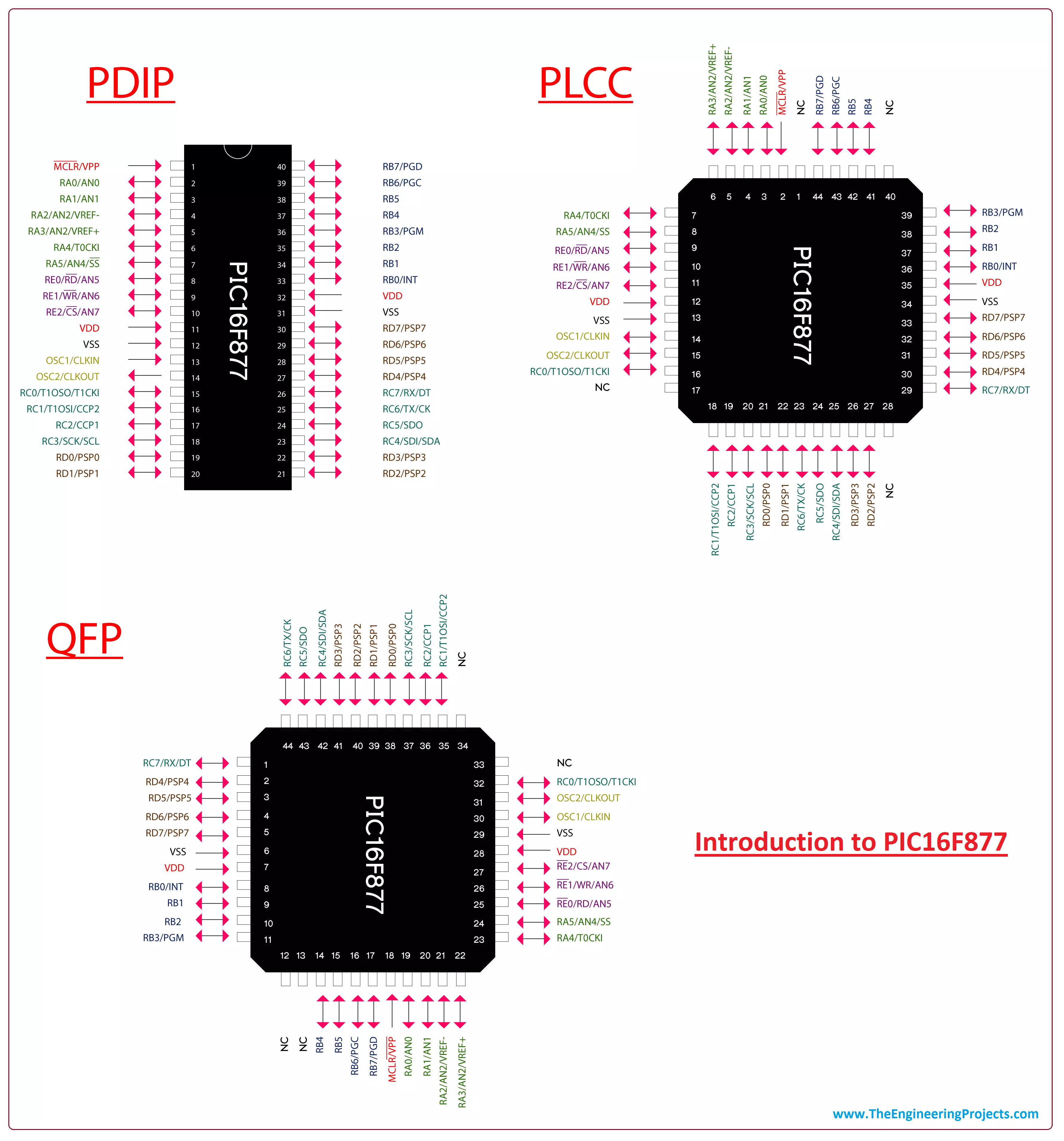
Hey Guys! Hope you are doing well. I am back to give you valuable information as per your technical needs and requirements. Today, I’ll unlock the detailed Introduction to PIC16F877. It is an 8-bit PIC microcontroller that comes with 40-pin interface (PDIP). It is based on Flash type memory. The High-Performance RISC CPU is incorporated inside the device that comes with only 35 single-word instructions, targeting mainly two types of instructions: single cycle and double-cycle. In this post, I'll cover each and everything related to PIC16F877: its features, pinout and pin description, main functions, memory interface, compiler and burner used and applications. Let's dive right in and get down to the nitty-gritty of this tiny device.

Introduction to PIC16F877

  • PIC16F877 is an 8-bit PIC microcontroller that is introduced by Microchip and is mainly used in automation and embedded systems.
It comes in three packages known as PDIP, PLCC, and QFN where the first one is 40-pin while other two come with a 44-pin interface.
  • It features 256 bytes of EEPROM data memory, 368 bytes of RAM, and program memory of 14K.
This microcontroller version incorporates CPU, timers, 10-Bit ADC and other peripherals that are mainly used to develop a connection with external devices.
  • The decent memory endurance around 1,000,000 for EEPROM and 100,000 for program memory, makes this device an ideal choice for many real-time applications.
The Universal Synchronous Asynchronous Receiver Transmitter (USART) is very helpful for developing serial communication with other devices.
  • Some internal and external reset features are added in the device that prevents the device from going stale, giving you a full authority to modify the controller as per your needs and requirements.
If automation is anything to go by, you cannot write off the importance of this little toy.

1. PIC16F877 Features

You have got a brief overview of the device. In this section, I have arranged the main features in a single table, making it easy for you to grab the main idea about the device. Let's have a look at the table.
CPU PIC
CPU Size 8-Bit
Total Number of Pins 40
I/O Pins 33
Analog Input 6
Flash Memory (Program Memory) 14 KB
SRAM 368 Bytes
EEPROM 256 Bytes
Timers (3) Timer0 Timer1 Timer2
Operating Voltage 4 to 5.5 V
Oscillator (Speed) up to 20 MHz
Manufacturer Microchip
Number of Ports (5) PORTA PORTB PORTC PORTD PORTE
Instruction Set 35 instructions
Capture/Compare/PWM Modules 2
Interrupts 14
A/D Converter 10-bit, 8 Channel
BOD (Brown Out Detection) Yes
Watch Dog Timer Yes
UART (Serial Communication) Yes
SPI Protocol Yes
I2C Protocol Yes
ICSP (In Circuit Serial Programming) Yes
DC Current for 3.3V Pin 50 mA
  • These features will help you understand the main characteristics of the controller and guide you in making a final decision before you intend to incorporate this chip into a certain project.

2. PIC16F877 Pinout and Description

In this section, we cover the pinout of the controller and a detailed description of each pin.
PIC16F877 Pinout
Following figure shows the pinout of PIC16F877.
  • This module comes in three packages known as  PDIP, PLCC, and QFP. The first one is mainly used for developing individual projects while other two are widely used in industrial applications.
PIC16F877 Pin Description
Following table shows the pin description of each pin. Some pins are capable to perform more than one function.
Pin# Pin Name Pin Description
1 MCLR' VPP Master Clear Active Low Reset Pin ICSP Programming Enable Pin
2 RA0 AN0 Digital I/O Pin Analog Input 0 Pin
3 RA1 AN1 Digital I/O Pin Analog Input 1 Pin
4 RA2 AN2 VREF- Digital I/O Pin Analog Input 2 Pin ADC Reference Input Voltage (low)
5 RA3 AN3 VREF+ Digital I/O Pin Analog Input 3 Pin ADC Reference Input Voltage (high)
6 RA4 T0CKI Digital I/O Pin External clock input for Timer0
7 RA5 AN4 SS' Digital I/O Pin Analog Input 4 Pin Slave Select input for SPI
8 RE0 AN5 RD' Digital I/O Pin Analog Input 5 Pin Read control for the parallel slave
9 RE1 AN6 WR' Digital I/O Pin Analog Input 6 Pin Write control for the parallel slave
10 RE2 AN7 CS' Digital I/O Pin Analog Input 7 Pin Select control for the parallel slave
11 VDD Voltage Supply Pin
12 VSS Ground Pin
13 OSC1 CLKIN Crystal Oscillator Input Pin
14 OSC2 CLKOUT Crystal Oscillator Output Pin
15 RC0 T1OSO T1CKI Digital I/O Pin Oscillator output for Timer1 External clock input for Timer1
16 RC1 T1OSI CCP2 Digital I/O Pin Oscillator input for Timer1 Output for Compare2 and PWM2, Input for Capture2
17 RC2 CCP1 Digital I/O Pin Output for Compare1 and PWM1, Input for Capture1
18 RC3 SCK SCL Digital I/O Pin SPI Module Synchronous serial clock input/output I2C Module Synchronous serial clock input/output
19 RD0 PSP0 Digital I/O Pin Parallel Slave Port for D0 with TTL input buffers
20 RD1 PSP1 Digital I/O Pin Parallel Slave Port for D1 with TTL input buffers
21 RD2 PSP2 Digital I/O Pin Parallel Slave Port for D2 with TTL input buffers
22 RD3 PSP3 Digital I/O Pin Parallel Slave Port for D3 with TTL input buffers
23 RC4 SDI SDA Digital I/O Pin SPI Data-In Pin I2C Data I/O Pin
24 RC5 SDO Digital I/O Pin SPI Data-Out Pin
25 RC6 TX CK Digital I/O Pin Asynchronous Transmit (USART) Synchronous Clock (USART)
26 RC7 RX DT Digital I/O Pin Asynchronous Receive (USART) Synchronous Data (USART)
27 RD4 PSP4 Digital I/O Pin Parallel Slave Port for D4 with TTL input buffers
28 RD5 PSP5 Digital I/O Pin Parallel Slave Port for D5 with TTL input buffers
29 RD6 PSP6 Digital I/O Pin Parallel Slave Port for D6 with TTL input buffers
30 RD7 PSP7 Digital I/O Pin Parallel Slave Port for D7 with TTL input buffers
31 VSS Ground Pin
32 VDD Voltage Supply Pin
33 RB0 INT Digital I/O Pin External Interrupt 0
34 RB1 Digital I/O
35 RB2 Digital I/O
36 RB3 PGM Digital I/O ICSP programming enable pin (Low voltage)
37 RB4 Digital I/O
38 RB5 Digital I/O
39 RB6 PGC Digital I/O ICSP programming clock, In-circuit debugger
40 RB7 PGD Digital I/O ICSP programming data, In-circuit debugger

3. PIC16F877 Main Functions

This PIC model is capable to perform many functions similar to other controllers in the PIC family. Following are the main functions of PIC16F877.
Timer
PIC16F877 comes with three timers known as Timer0 (8-bit), Timer1(16-bit) and Timer2 (8-bit). These timers can be used as a timer as well as a counter.
  • The timer mode is mainly used to increment the instruction cycle while the counter mode plays a vital role to increment the rising and falling edge of the pin.
All three timers contain internal and external clock select capability.
USART
PIC16F877 incorporates a USART (Universal Synchronous and Asynchronous Receiver and Transmitter) module that is mainly used to establish the serial communication with external devices.
Watchdog Timer
PIC16F877 comes with a built-in watchdog timer that takes the controller back to reset position if the program hangs up during compilation or gets stuck in the infinite loop.
  • It is nothing but a hardware timer that produces a system reset if the main program fails to periodically service it.
It is advised to reset this timer to the initial value after every 3 instructions in order to avoid it going to zero value in normal conditions.
  • The Watchdog Timer can be controlled only through configuration bits. It comes with its own RC oscillator for maximum reliability.
Brown Out Reset (BOR)
The BOR function is a very remarkable addition that puts the device in reset condition once the Vdd (voltage supply) drops below a brownout threshold voltage.
  • If the Power Up Timer is kept enabled, it will create the delay for returning the device from a BOR function. The BOR mode can be configured both ways: BOREN settings in a register or using programming.
The multiple voltage ranges are provided to secure the chip if the power drops at the voltage supply line.
In-Circuit Serial Programming
In-circuit serial programming (ICSP), also called In-system programming (ISP), is a function that allows the chip to be programmed in the required project after installation, setting you free from plugging and unplugging the device in the project over and over again.
Master Clear Reset (MCLR)
The MCLR pin serves as an external reset for the chip. This pin is independent of the internal resets and is activated by keeping this pin at a LOW value.
  • The MCLRE configuration bit is mainly used to disable MCLR input and the noise filter is included in the MCLR executing process that allows to detect and remove the small pulses.
Power On Reset
Power On Reset function is a very useful function that resets the controller and prevents it from malfunctioning. When the module is powered on, the power-on reset will start the module from scratch once the Vdd raises above a certain threshold value.
  • The Power Control (PCON) Register comes with flag bits that help to differentiate between a Power-on Reset (POR), a Watchdog Reset(WDT) and external MCLR Reset.
SPI Communication

Serial Peripheral Interface (SPI) is a remarkable function of the chip that is commonly used to send data between microcontrollers and small peripherals such as sensors, shift registers, and SD cards.

  • It comes with separate clock and data lines, layered with a select line to choose the device for communication.
I2C Communication
The I2C is a two-wire interface communication that comes with two main lines known as SDA and SCL where former is s serial data line that carries the data and later is serial clock line that is used to synchronize all data transfers over the I2C bus.

4. PIC Compiler

  • PIC compilers and burners are used for different purpose. The former is a software used to write the desired code for the module while later is used to transfer and burn the code on the module.
There are various compilers used for the PIC controller and MPLAB C18 Compiler is an official compiler main developed for the PIC modules. You can get this compiler online from the Official Microchip Site.
  •  MikroC Pro For PIC is a third party software and is a good replacement for PIC standard compiler.
  • These Top 3 PIC C Compilers give you the flexibility to choose from and pick any compiler as per your needs and demands.
The code written in the compiler generates a hex file which is then transferred to the microcontroller using a burner.
  • The PICKit3 is a standard PIC burner for PIC controllers. Other burners are also available in the market but PICKit3 is mostly preferred for the PIC controllers.

5. PIC16F877 Memory Layout and Working

Memory, as the word suggests, is used to store a number of instructions inside the controller. It is mainly divided into three major types: Program Memory (Flash Memory) Data EEPROM Data RAM Let’s get down to the main features of each memory.
Program Memory
The Program memory, also known as ROM memory or Flash memory, stores the number of instructions permanently.
  • It comes with a memory space around 14K and is independent of the power supply i.e. have the ability to store information in the absence of main power supply.
Data EEPROM
The EEPROM Data Memory is similar to ROM memory with one exception i.e. the instructions in EEPROM can be controlled and modified during the controller operation.
  • The EEPROM incorporates memory space around 256 bytes and is mainly addressed by multiple control registers.
Data RAM
RAM memory, also known as volatile memory, stores the program temporarily and is dependent on the power supply. It comes with a memory space around 368 bytes  and is mainly classified into two main parts called General-purpose registers (GPR) Special-function registers (SFR)
  • These registers are spread across the multiple banks and are the data holding places that can hold instruction, storage address, and any kind of data ranging from an individual character to bit sequence.
General purpose registers are implemented as a static RAM and can be easily accessed by File Select Register. They store any modified or random value in the processor and are located on the upper side of banks.
  • On the other hand, Special function registers are located on the lower side of the banks and are used to control the peripheral functions, covering the first 32 locations of each bank.
When reduction and decent code execution is required, some Special Function Registers from one bank are mirrored and placed in another bank.

6. PIC16F877 Block Diagram

The following figure shows the block diagram of PIC16F877.
  • PIC16F877 comes with five ports where each port contains 8 pins except the E port that comes with 3 pins.
  • It is important to note that higher order bits are related to the STATUS register

7. PIC16F877 Projects and Applications

PIC16F877 comes with a variety of applications with the main aim to drive automation in the relevant project. Following are some major applications it can be used for.
  • Student projects for motor controlling and sensor interfacing
  • Health and security systems
  • Central heating projects
  • Embedded system
  • Gas sensor projects
  • GPS projects
  • Serial Communication
  • It is widely used in home and industrial automation
  • Production of temperature data logger

8. Why Use PIC MicroControllers

  • Earlier, if you were aiming to design the automation project, you'd need a bunch of wires and a plethora of electrical components, that would not only cost you more but making your project heavy with more space requirement. These PIC controllers prove to be a lifesaver for your technical needs requiring minimum circuitry.
  • These controllers come with a user-friendly interface and easy onboard architecture that requires little or no prior skills before getting familiar with the chip.
  • PIC controllers have a leg over other Atmel controller like 8051 due to their higher processing speed and efficiency.
  • They are very handy in terms of consuming minimum power consumption that makes this controller an ideal choice for the projects where power limitation is a major concern.
That’s all for now. I hope I have given you everything you needed to know about PIC16F877. If you are unsure about anything you consider I have left unsaid about this chip, you can ask me in the comment section below. I’d love to assist you in any way I can. You are most welcome to keep us updated with your valuable suggestions, we plan our content strategy based on them, so keep them coming. Thanks for reading the article.

Introduction to 1n4738a

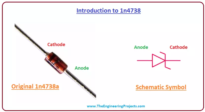
Hi Guys! Hope you are doing well. I am back to give you nuggets of valuable information related to engineering and technology so you can excel and grow in your relevant field. Today, I'll unlock the detailed Introduction to 1n4738a. It is a zener diode that comes with high power rating and is mainly used in stabilizing and clipping circuits. The zener diode is slightly different from regular diode as former can conduct in both directions while later conducts in one direction only. It is available in double slug construction with corrosion resistant surfaces, helping to operate it under high temperature and pressure. I'll try to cover each and everything related to this diode, so you don't have to grapple your mind surfing the whole internet and find all the information in one place. Let's jump right in and get down to the nitty-gritty of 1n4738a.

Introduction to 1n4738a

1n4738a is a zener diode that comes with an ability to conduct in both directions. It is a high power device mainly used in stabilizing and clipping circuits.
  • This zener diode features maximum lead temperature for soldering around 230 C. It comes with a zener voltage around 8.2 V and external leads are attached with the body, helping thru-hole mounting.
This zener diode is nothing but a p-n junction diode with current capability conducting in both directions i.e. forward direction and reverse direction, featuring very effective working characteristic with a power dissipation of around1300 mW.
  • You can not make it work in a reverse biased condition unless reverse breakdown voltage is achieved before the normal device operation.
It is important to note that the voltage drop across the zener diode doesn’t change over a wide range of voltages, which makes it a valuable pick for voltage regulation applications.
1n4738a Working
This zener diode is similar to a normal diode when it operates in a forward biased condition. However, working in a reverse biased condition is a totally different story that will only take place when the reverse voltage reaches the breakdown voltage, making diode flow current from cathode to anode.
  • When a wide range of applied voltage is applied, the corresponding current reaches to a maximum point and strive to stabilize itself after some time. This process will make the diode working as a voltage stabilizer.
The Voltage Breakdown state can be achieved in two ways: using Zener Breakdown Effect or Impact Ionization. These mechanisms start to happen at 5.5 V and don’t require different circuitry for a flawless working process.
  • However, the temperature coefficient sets them apart from each other as Zener effect comes with a negative temperature coefficient while the impact ionization features a positive temperature coefficient. And both effects cancel each other at 5.5 V, helping zener diode to gain the stable and reliable state over a wide range of temperatures.
1n4738a Absolute Maximum Ratings
Following figure shows the absolute maximum ratings of 1n4738a.
  • If stresses are exceeded above these absolute maximum ratings, they can damage the device.
  • Similarly, if stresses are applied for the extended period of time, they can affect the device reliability.

Applications

This zener diode is widely used in consumer electronics. Following are the major applications it can be used for.
 As a Waveform Clipper
Zener diode serves as a waveform clipper when connected in series. In this case, it will clip the waveform from both ends of the cycle i.e. positive end and a negative end of the cycle. In zener diode, the signal we get at the output comes with some major voltage spikes. However, if diodes are connected in series, they impede the diode from producing spikes, eventually modifying the output signal with a smooth waveform.
As a Voltage Shifter
  • Zener diode is widely used as a Voltage shifting device.
  • As a voltage shifter, it strives to make both output and breakdown voltage equal in magnitude.
That’s all for now. I hope I have given you everything you needed to known about 1n4738a. If you are unsure or have any question, you can approach me in the comment section below. I’d love to help you the best way I can. You are most welcome to feed us with your valuable suggestions, they help us provide you quality work. Thanks for reading the article.

Introduction to 2sa1265

Hi Guys! Hope you are doing well. Welcome you onboard. Today, I'll unlock the detailed Introduction to 2sa1265 which is a PNP transistor mainly used for power amplifier applications and proves to be an ideal choice for 70W high fidelity audio frequency amplifier output stage applications. This PNP transistor falls under the category of Bipolar Junction Transistors where two charge carriers i.e. electrons and holes take part in the conduction process, however, holes are major charge carriers in the PNP transistors, unlike NPN transistors where electrons are the major charge carriers.
  • BJTs are different than that unipolar transistors like JFETs as former is the current controlled device and later is a voltage controlled device. Both are used in different areas ranging from consumer electronics, industrial to commercial applications.
In this post, I'll try to cover some basic details related to 2sa1265, its main features, pinout, working, and applications. Let's jump right in.

Introduction to 2sa1265

2sa1265 is a PNP transistor mainly used for power amplifier applications. It is composed of three layers: two P doped layers and one N-doped layer which is sandwiched between the other two layers.
  • This transistor contains three terminals known as an emitter, base, and collector. The base terminal is more negative than the rest of the terminals.
These terminals come in different size and doping concentration. The emitter terminal is highly doped and features 100% of the transistor current while the base terminal is lightly doped and controls the conduction inside the transistor. The collector terminal is moderately doped and is bigger in size than other terminals.
  • The PNP transistor won't be conducting if there is no supply voltage at the base terminal, however, when a voltage is applied at the base terminal it draws current which is then used to control large current at other terminals.
It is important to note that, both NPN and PNP are used for amplification purpose but voltage polarities and current directions are reversed in both transistors i.e. in NPN transistor current flows from collector to emitter and in PNP transistor current flows from emitter to collector.
  • The 2sa1265 PNP transistor comes with two PN junctions i.e. emitter-base junction and the collector-base junction where former is forward biased and later is reverse biased.
Under normal conditions, the PNP transistor comes with voltage drop out of 0.7 V, so the voltage at the base side must be 0.7 V less than the voltage at the emitter side for making emitter-base junction a forward biased.
2sa1265 Pinout
Following figure shows the pinout diagram of 2sa1265.
  • In the case of PNP transistor, emitter voltage is much larger than collector voltage which is necessary for the transistor to conduct.
  • The transistor turns on as a small current starts flowing from emitter to base terminal.
2sa1265 Circuit Diagram and Working
Following figure shows the circuit diagram of 2sa1265. When a voltage is applied at the base terminal, the majority of holes move from the emitter and get diffused into the base terminal, combining with the electrons.
  • As the base is very thin and lightly doped it cannot hold the number of electrons for a maximum period of time, ultimately allowing the electrons flow from base to collector terminal.
In many amplification applications, NPN transistors are preferred over PNP transistors because conduction carried out by the movement of electrons is preferable over the conduction carried out by the movement of holes.
  • Combination of PNP transistor with NPN transistor is widely employed for the development of the power amplifier circuits. Power B amplifiers are a great example of this amplifier circuits where both PNP and NPN transistors are joined together to produce a high amplification cycle.
2sa1265 Absolute Maximum Ratings
Following figure shows the absolute maximum ratings of 2sa1265.
  • These are the stress ratings defined by the manufacturer. If you want the device to be running properly without any damage and undergoes a longer life, you must follow these operating conditions.
  • If these ratings are provided for the larger amount of time than the normal operating condition, they can affect the device reliability which may cause more damage in the later stage once your electronic project has been executed.
Applications
  • It is used in power amplifier applications.
  • An ideal choice for 70W high fidelity audio frequency amplifier output stage applications.
That's all for now. I hope I have given you everything you needed to know about 2sa1265. If you are unsure or have any question, you can ask me in the comment section below. I'd love to help you according to the best of my knowledge. Thanks for reading the article.

The Ultimate Ways to Lower Manufacturing Costs

Hey Friends! Hope you are doing well. I feel pleasure to keep you updated with valuable information related to engineering and technology. Today, I'll discuss The Ultimate Ways to Lower Manufacturing Costs. Every business will definitely need to offer quality products at affordable rates not only to remain competitive but to maximize revenues as well. But, what to do if your customers are not ready to pay a good amount for your products? Trimming the manufacturing costs down without compromising the quality can be a great idea for you to enjoy good profit margins in order to reach your business objectives and goals.

The Ultimate Ways to Lower Manufacturing Costs

Countless ways to lower manufacturing costs are available but you shouldn’t be wild with useless manufacturing cost-cutting ideas that may ruin your goodwill in the market instead of growing it. Following are some ultimate ways to lower manufacturing cost that will keep you alive in the competitive market and help you grow your business skyrocket.
Start with Assessment
Since thoroughly conducted assessment is considered as the very first step taken to deal with a problem or issue, you should do the same to reduce manufacturing costs ultimately.
  • By taking a deep look into the whole manufacturing process and strategy, you will be able to bring improvement in things accordingly. By doing so, you can set yourself up for a long-term success.
Prioritize ROI when Investing in Latest Solutions
During the assessment, if you have found most of the things that can be revised for better production processes by cutting the costs down, maximum return on investment should be your priority to invest business money in the right manufacturing solutions.
  • You will need to think about the long-term business benefits instead of first-time costs as it can help you save the business money in the long run.
Seek Improvement Ideas from Staff
Your employees and staff can be the best source of fertile manufacturing cost-cutting ideas. Business experts and consultants usually talk with the employees to inquire about things that can help them make profitable decisions and you should be doing the same. Staff and employees carrying out the manufacturing process are the individuals who continuously go through the process and can give you ideas regarding how things can be better than before.
Find Cost Savings in Energy Reduction
Fuel or energy can be one of the highly expensive components of the overall manufacturing process and shifting to a less expensive energy solution can be great for your business to diminish its production or manufacturing costs ultimately.
  • For example, if you can consume gas instead of electricity to carry out manufacturing procedures without compromising the quality, then be quick to shit if it contributes a lot to your manufacturing cost-cutting strategy.
Tweak Your Design
Getting attached to the real product design or idea is natural but the designing decisions you take at initial usually are not best and profitable as well in long run.
  • For instance, you may have selected the necessary materials and other elements without understanding the cost projections and many other things. This is the point where a reliable prototype manufacturer can make things easier for you by creating the best prototype of your idea or product design.
In this way, you will be able to opt up for different, less expensive and quality raw materials and other components to lower the manufacturing costs and increase profit margin ultimately.
Reconsider Old Ideas
You can also find some great cost-cutting ideas by going back and looking at the previous ideas proposed by fellow businessmen or experts. Some of the old ideas might be working, for now, to help you save money in terms of reduced manufacturing overheads.
  • If there are more than a few great ideas that make sense, then be quick to implement in order to lessen manufacturing cost per unit without losing the quality.
Automate Where you Can
Business process automation is something most common in this digital world that not only ensures accuracy but also allows a business or company to produce more in less time even without using more resources.
  • Advanced technology is always there to help you produce things with no or fewer human interaction and with enhanced accuracy that can cause less use of labor and employees.
Elimination of manual manufacturing processes will not only aid you to produce high-quality products but will also save the business money in terms of fewer labor costs.
Sell Scrap to Earn
Your trash can be useful for someone else, so always sell your scrape and useless material to other vendors in order to add more money in your manufacturing budget or to purchase more raw materials without using business accounts.
  • You should also check with your current vendors or suppliers if they purchase scrap because they can pay you well.
Negotiate with Suppliers and Vendors
When it comes to making purchases from vendors and suppliers, ask for the offers or the best rates for bulk purchases because a little bargain can save a lot for your business.
  • Instead of accepting the first price presented, ask them if they can do a favor for you by providing the desired materials or products on discounted rates.
That's all for today. I hope you have found this read valuable. If you have any question, you can ask me in the comment section below. You are most welcome to keep us updated with your valuable suggestions, we shape our content strategy based on them, so keep them coming. Thanks for reading the post.

Introduction to JK Flip Flop

Hi Guys! Hope you are doing well. I am back to keep you updated with valuable information related to engineering and technology. Today, I'll discuss the detailed Introduction to JK Flip Flop. It is a flip-flop, also known as a latch circuit, that can be either active-high or active-low based on the signal applied. It is an improved version of the SR Flip Flop and prevents the circuit from going in an invalid state. As the name suggests, it helps the circuit toggle between two states.
  • The JK flip-flop is named after his inventor known as Jack Kilby from Texas Instruments. The JK Flip-flop is also widely known as a  programmable flip-flop as it can disguise other flip-flops based on the inputs applied.
There is a slight difference between Flip-flop and latch. Don't you worry, we will figure it out later in this post. Rest assured, both are nothing but a data storage element mainly used in communications, decoders, multiplexers, and registers. In this post, I'll cover each and everything related to JK Flip Flop, so you don't have to wrestle your mind surfing the whole internet and find all the information in one place. Let's jump right in.

Introduction to JK Flip Flop

JK Flip Flop is a universal flip-flop that makes the circuit toggle between two states and is widely used in shift registers, counters, PWM and computer applications. Before we nail down the details of JK Flip Flop, we must know what is Flip Flop.
  • Flip Flop comes with two stable states and is mainly used to store the state information of any circuit. The output of the flip-flop is directly related to the input applied. When you modify any of the applied input, it directly influences the output state of the device.
In engineering circuits, most of the devices need to store information using Set or Reset, HIGH or LOW which ultimately written in the form of zeros and ones.
  • We use language to collaborate with each other, similarly, electronic devices need some language pattern to collaborate with other electronic devices. They understand a language in terms of ones and zeros where former represents the HIGH state and later represent the LOW state of the circuit.
The circuits that come with a toggling nature whose outputs depend on the present input and the sequence of past input values are known as Sequential Logic Circuits.
JK Flip Flop Symbol and Logic Table
Following figure shows the symbol of Flip-Flop circuit. The clock signal and input are closely related to each other. When the clock signal is active LOW, the input signal won't be affecting the output state. The input will only get active when the clock is active HIGH which serves as a control signal of the circuit. Based on the applied inputs, the output will be generating two stable states.
  • The J and K are the inputs and Q is the output state of the flip-flop where Q' represents the inverted output state. In the presence of the clock signal, the output changes its state based on the applied inputs, producing a toggling function when both inputs are HIGH.
Following figure shows the logic table of the JK Flip Flop. When both inputs are active HIGH, the output starts toggling between the two states. This is the reason JK Flip Flop is widely considered as an astable device.
Difference between SR and JK Flip Flop
Two flip-flops are known as JK Flip and SR Flip are widely used in electronic applications. Using the SR flip-flop when both inputs are high, will generate an invalid condition. On the other hand, JK Flip Flop extensively removes the invalid condition, when both inputs are kept HIGH, by toggling the output alternatively between two states.
  • The JK Flip Flop is nothing but an improvised version of SR Flip Flop, where an undefined condition is avoided that may create a gross impact using the SR Flip Flop.
Following figure shows the logic table of SR Flip Flop. You can see, when both inputs are 1, the circuit goes to the invalid state. Note: The SR flip-flop is also known as a 1-bit memory, as it comes with an ability to store the input pulse even after it has been passed.
Difference between Flip Flop and Latch
The basic difference between a latch and a flip-flop is a clocking process. The latch is asynchronous where outputs are drastically influenced by the slight change in inputs.
  • A flip-flop is synchronous and edge-triggered that changes its state based on the control signal (clock signal) as it goes from HIGH to LOW and LOW to HIGH conditions.
In SR Flip Flop, the output Q would be high as you set S active HIGH and eventually Q’ will be low, producing the asynchronous result. On the other hand, SR latch is synchronous where output changes as you give an active clock signal.
  • In other words, we can conclude, both latches and flip-flops are circuit element where the output depends on both: the current input and previous input. The flip-flop has a clock signal while the latch is deprived of it.
The Latch is mainly divided into two types Active High Latch Active Low Latch

In an Active-high latch, the inputs are connected to ground, activating the latch by applying the HIGH signal on either of the inputs. If the SET input goes HIGH, it will keep the output HIGH even after the SET input goes LOW. The output will go LOW only when the RESET input turns HIGH.

And in an Active-low latch, the inputs are kept HIGH, activating the latch by applying the LOW signal on either input. When the SET input turns LOW, the output will go HIGH. The output remains in HIGH condition until the RESET pin goes LOW.

Applications
JK Flip Flops is widely used in electronic circuits with the main aim to store the state information of the device. Following are the major applications it can be used for.
  • Shift Registers
  • Data storage
  • Data transfer
  • Counters
  • Frequency Dividers
  • Bounce elimination switch
  • Storage Registers
That's all for now. I'll be writing more articles related to some basic circuits used in engineering. If you have any question, you can ask me in the comment section below. I'd really appreciate if you have something to add in this post that has been left unsaid. Based on your feedback and suggestions, we shape our content strategy, so keep them coming. Thanks for reading the article.

Introduction to ULN2803

Hey Guys! Hope you are doing well. I always take pleasure to keep you updated with valuable information related to information and technology. Today, I'll discuss the detailed Introduction to ULN2803 which is a relay driver that comes with a high-voltage and high-current Darlington transistor array. In order to obtain higher current capability, the Darlington pairs are connected in a parallel configuration. The component is incorporated with eight NPN Darlington pairs, featuring high-voltage outputs with common-cathode clamp diodes that are directly related to switching inductive loads. Each Darlington pair features a decent amount of collector-current rating i.e. around 500 mA. You must have a look at ULN2003 which is almost similar to this IC but comes with 16 pins and can handle 7 relays at a time. In this post, I'll cover each and everything related to this driver IC: its main features, pinout, working, and applications. Let's dive in.

Introduction to ULN2803

ULN2803 is a high-voltage and high-current Darlington transistor array and is mainly used as a relay driver with an ability to handle 8 relays at a time. It comes with a collector-emitter voltage around 50 V and input voltage residing at 30 V.
  • Before we move further, we must know what is Darlington transistor? It is commonly known as Darlington pair which is nothing but a combination of two bipolar transistors featuring a compound design and is connected back to back where current amplified by the first transistor is again amplified by the second one.
This shape delivers a much higher current gain as compared to each transistor taken separately. It works on the simple amplification principle happening in the regular transistor where a small base is used to make the pair switch for higher switching currents.
  • This Darlington transistor mainly operates at 5V  and is based on TTL (Transistor-Transistor Logic) and CMOS (Complementary Metal Oxide Semi-Conductor).
The NPN transistors forming arrays are useful for both: interfacing between low logic level digital circuitry and achieving the higher current/voltage requirements in a wide range of applications including printer hammers, lamps, relays, consumer and industrial applications.
  • The device shows open–collector outputs and freewheeling clamp diodes that turn out to be very handy for transient suppression.
ULN2803 Pinout
Following figure shows the pinout of ULN2803. It comes with 8 input pins and 8 output pins.
Pin Configuration
Pin number from 1 to 8 is a Channel 1 through 8 Darlington base input while pin number from 11 to 18 is Channel 1 through 8 Darlington base output. Similarly, 9 and 10 pins are ground and common cathode node (Vcc) respectively. It is important to note that common emitter is shared by all the channels. Following table shows the pin configuration of ULN2803.
ULN2803 Logic Diagram
Following figure shows the logic diagram of ULN2803. It is a visual representation and arrangement of how the diodes are connected in the component. Following figure shows the schematic diagram of each Darlington pair. You can see how the resistors and diodes are connected with each other. And the amplified output of one resistor is further amplified by the second resistor, giving a whopping amount of current gain which is difficult for the individual diode to achieve if incorporated separately.
ULN2803 Absolute Maximum Ratings
Following figure shows the absolute maximum rating of this component. These are the stress ratings which if exceed from absolute maximum ratings, can damage the device at large, ultimately affecting the overall nature and performance of the project.
  • Similarly, if these ratings are applied for the maximum period of time above normal operating conditions they can affect the reliability of the device.
Steps and measurements taken in the early stages of your project can save you from the atrocities of spending more in case the electronic circuit gets affected.
  • It is preferred to check these ratings before placing the device in the circuit and make sure these ratings are quite in line and match exactly as defined by the manufacturer.
Applications
ULN2803 comes with a variety of advantages with a common application as a relay driver. Following are some major applications of this Darlington array.
  • LED display
  • Hammer Drivers
  • Motor driver circuits like DC Motors or Stepper Motors
  • IP Camera
  • Lamp Drivers
  • Stepper Motors
  • Logic Buffers
  • Line Drivers
  • HVAC Valve and LED Dot Matrix
This is all for today. I hope you have found this read valuable. If you have any question, you can approach me in the comment section below. I'd love to help you the best way I can. Your feedback and suggestions are a valuable asset for us. Based on them, we develop our content strategy, so keep them coming. Thanks for reading the article.

Common Engineering Problems and How to Alleviate Them

Hi Friends! Hope you are doing well. I am back to update you with some nuggets of valuable information that keeps your innovation alive, helping you think out of the box. Today, I'll highlight the Common Engineering Problems and How to Alleviate Them.  All men are born equal while some of them opt to become an engineer. The field that looks enticing for almost everyone and makes them feel captivated with the thought, if you become engineer, you'd be a billionaire at some point of your life. I'm not sure if you can make it happen or not, but you need to understand the common problems before you aim to join the engineering field. Let's jump right in and get to the point.

Common Engineering Problems and How to Alleviate Them

When nature decides the gender of the babies, our parent strives to plan their future. If you born in a traditional family, you are left out with three options to choose as a career
  • Doctor
  • Engineer
  • What your parents want
You get loads of marks in high school, clear entry test, apply for admission, result rolls out, and congrats you get admission in the university you aimed for. Now the real manipulation begins. University days are awesome, not for everyone, but a person who knows how to manage both educational and social life. More or less, engineers live a painful life, working on daunting lengthy assignments and presentations with no clue, all these university prerequisites are far less than the atrocities of professional life.
Punch in the Stomach
Some students get too high GPA, somewhere around 3.999 (+0.11), that they feel overwhelmed by the question right after their graduation – you are passed out with tons of marks, why are you jobless by now? This question looks like a punch in the stomach, giving you no flexibility to defend yourself. Teaser: It is better to get a low GPA and remain jobless than getting high GPA with no job.
Why ain’t you doing a Field Job?
As you remain jobless for two, three years after graduation, you feel shy to introduce yourself as an engineer with the fear, they are going to ask about your job. God forbid if you get the job anyway, but not in your relevant field, brace yourself with the taunt, if you have done engineering, why ain’t you doing the job in your field?

Some Common Engineering Fields

Mechanical engineers: They are amazing. Some confuse them with mechanics. They struggle hard in college with the notion, there will be a lot of girls in the engineering field. And when they get admission, they come to know, only 3 or 4 girls are there in the class, left them calculating how much boys are reserved for each girl. Electrical engineers: They are magical. And when they fail to fix any home appliance, they go into drastic inferiority complex, thinking, if they worth less than an electrician? Nonetheless, thanks to these engineers, without them we would be living in the darkness and no bunch of electricity was available (if we ignore few countries) to decorate and flavor up our homes, shops and picnic places. If you are an electrical engineer and reading this post right now, you may have to develop a project quite often with PCB as the main part of it. You can pick PCBWay in order to fill your technical needs for quality PCB that will help you design the project with thick copper on the surface, providing a solid and coherent interface and helps join all components on a single board. Mechatronics Engineers: Google is the second best tool that knows everything, Mechatronics engineers still stand first. They are a jack of all trades but master of some. Mechatronics is a combination of mechanical and electronics with little ingredients of every field including computer, civil, architecture, transportation, chemical, and petroleum engineering with some taste of fashion designing, law, C.A, health and fitness and biomedical. They can be a good fit for any field. Apart from doing their field job, if there are some, they are good at babysitting, traveling, adventure and storytelling. Whenever they appear for any job interview, knowing the job offer is purely related to the certain field, they present themselves expert in an exactly opposite niche. If the company offers an electrical job, they appear in the interview anyway, stating they have a profound knowledge in Thermodynamics, let alone designing and manufacturing and overhauling Ford Car Engines.

How to Alleviate Common Problems

Only engineers can truly understand the atrocities they face in their lifetime. Every person comes with a unique nature and mindset, not every advice stands fit and resonates with everyone. However, with an ability to comprehend some common rules and real understanding, everyone can fix their problems, let alone engineers.
Skill matter, GPA doesn’t
Needless to say, if you are scoring 2.99 GPA, you are doing well. I’m sorry for the thetas but what is the point of stressing out for four years, if you are going to get paid the same or sometimes less than average students. Remember, skill outperforms memorizing talent in most of the cases. Instead of cramming the course, you must aim for boosting up your skills. It happens, when student pass out and complete graduation, they have no idea about the skills they are good at. In university, they learn a bundle of software with no mastery in any of them. However, if they learn only one software like a Pro, they surely have something to offer and market themselves as a brand in particular skill.
Money is Something, not Everything
Lack of career counseling is the major issue Graduate Students face right now. Yes, money does matter. It is something, if not everything. You spend a full four years in university, thinking you are going to get paid a bunch of dollars. And all these dreams gone to dust when you know, no company is ready to pay you enough so you can enjoy and spend life with full liberty without the fear of getting stuck with empty pocket at the end of the month.
Put your Health First
I know some of the friends, if we ignore 90% of them, are making good money, with no intention, if their health is put on hold. Money is necessary, health comes and goes, right? Wrong! Adopt the job what makes you feel happy at the end of the day. If you are earning too much in a job that makes your health bleed, then you are playing a risky bet. Protip: There is a scope in every field as long as you know how the knack for time management and basic knowledge to present things from your boss’s perspective and what makes him feel good. Presentation of works bears more value than the actual work itself. The crux of this read: No matter what engineering you do, all it boils down how much are you making in the end. If you are making the handsome amount, there is no need to wrestle your mind getting a field job. That's all for today. I hope you have got something valuable out of this read. You are most welcome to keep us updated with your valuable feedback and suggestions, they help us provide you quality work so you keep coming back for what we have to offer. Thanks for reading the article.

Introduction to RS 232

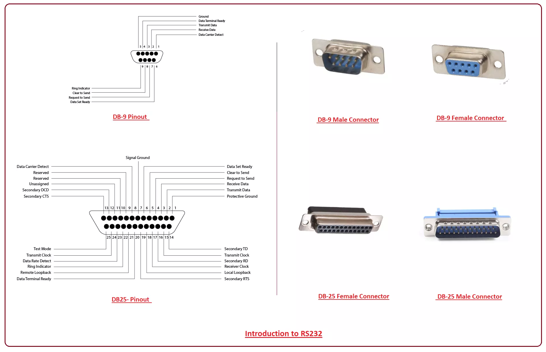
Hello Friends! Hope you are doing well. I am back to give you a daily dose of valuable information. Today, I'll discuss the detailed Introduction to RS 232 which is a standard communication protocol mainly used for serial communication between two devices. It was first introduced by the EIA (Electronic Industries Association) in 1960 to provide a pathway for connecting one device with other peripheral devices for flawless digital communication. It is true, that the inception of USB has grossly reduced the need for RS232 protocol, still, we can't brush off its significant importance in some industrial applications where Programmable Logic Controllers and Computerized Numerical Control Equipment are specifically programmed using RS 232 connectors which is nothing but an interface between DTE (Data terminal equipment) and (Data communication equipment). Don't worry about these abbreviations, I'll come to them later. In this post, I'll walk you through the basic concept of RS 232, why it is used and what are its main advantages and limitations. Let's dive in and explore the main features of the RS 232 protocol.

Introduction to RS232

RS 232, recently known as TIA 232, is a recommended standard protocol for serial data transmission between the electronic devices. It mainly works on three line signals: a transmission line, receive line and ground.
  • The transmission line is mainly used to send the data serially from one end and receive line accepts the data from the other end while the common ground is used for devices.
Initially, it was very difficult to devise the clear protocol to send the data from one end to another. This led to the inception of the RS 232 protocol, revitalizing the communication industry with the main purpose to keep both ends of the connecting device under the same roof where they can accept, understand and communicate in the same language. The RS 232 is mainly categorized into two systems: DTE and DCE. DTE is a data terminal equipment such as a computer that handles the communication with some control functions and plays the main part of the station. Similarly, DCE is a data circuit-terminal equipment that is placed on the other end of the station and understands data being communicated from the DCE equipment. The DCE system incorporates male DB connectors while the DCE system comes with female DB connectors.
  • RS232 data is bi-polar in nature, indicating an "ON or 0-state (SPACE) condition" if a voltage is around 3 to 12 V and features an "OFF" or 1-state (MARK) condition if voltage ranges from -3 to -12 V.
It is important to note that, most of the companies have reshaped the internal structure of the recent computers where they still indicate an OFF state at the zero voltage level, all the while ignoring the negative voltage. Similarly, the "ON" state is not necessarily dependent on the highest voltage level and can be achieved with much less voltage around 5V. Serial communication is mainly based on logical terms and RS232 transfers one bit at a time in the stream of ones and zeros which at the other end eventually get converted back to bits. There are eight bits in one byte.
  • The duration at which the required signal stays in the particular state is dependent on the baud rate. The communication carried out in a RS 232 protocol is measured in baud - A number of bits transferred per second i.e. 1000 baud indicate 1000 bits per second.
There are other parameters that must be set up before the data transmission: Length of the byte, Parity and magnitude of stop bits. This length of the signal can be reserved anywhere from 5 to 8 bits. The second parameter is important. Partiy mainly comes with five options
  • Even
  • Odd
  • Mark
  • Space
  • None
Even parity indicates the last data bit transmitted will be a logical 1 if it contains an even number of 0 bits. Similarly, Odd parity will be showing that the transmitted data is termed as logical 1 if it comes with an odd number of 0 bits. And MARK and SPACE parity will be representing that the last transmitted data bit will be logical 1 and 0 respectively. The last parameter is a number of stop bits and its value is set as 1 or 2. Transmission Capability RS-232 can perform transmission at data rates up to 20 Kbps with distance range capability around 50 ft. It all depends on the capacitance of the cable. The low capacity cables can transfer data up to 1000 ft while cables with high capacitance can transfer data at the lower distance.
  • As mentioned earlier many computers don't come with RS 232 port anymore, therefore we need to add USB-to RS 232 converter externally in order to make them compatible with RS 232 peripheral devices.
Although excessive use of RS 232 becomes obsolete, they are still used in low speed wired data connection and point-to-point networking equipment with short range capabilities.
Communication Process
The communication is simply based on the transmission and receive protocol and a total of 9 pins are involved in carrying out the complete transmission. The following figure shows how the data is transmitted over the terminal. Mainly the communication is laid out between DTE and DCE terminals over the mutual agreement for required data transfer. The RTS pin shows the desire to send data to another terminal. As it turns ON, it indicates the DTE terminal is ready to transfer the data. The data will be transmitted gradually over the line without any resistance if CTS pin from the other is activated and grants permission to DTE for data transfer.
  • The CD pin represents the current status of the RTS pin. If CD pin remains turned OFF, it will show the DTE terminal is not ready to send data over the channel. Similarly, turning it ON will be showing the DTW desires to send data and looking for permission from the other end.
Once the permission is granted, two other pins RD and TD come into play where former is used to receive data from DCE terminal and later is used for transferring data from DTE to DCE terminal.
  • The DTR pin must be turned ON before both terminals are ready to communicate with each other. Actually, DTR (Data Terminal Ready) will be indicating that entire arrangement from both terminals is adequate and matches with the required protocol for data transfer. It serves as a go-ahead signal for the communication.
Connector Pinout
Following figure shows the configuration of DB 25 connector. Following figure shows the pin configuration of the DB-9 connector.
  • DB-9 and DB-25 connectors offer the outstanding quality and reliability for a number of serial and parallel (IEEE 1284) applications.
Types of Serial Communication
There are two main types of serial communication. Half Duplex Full Duplex Half Duplex, as the name suggests, transfers the information in one direction only. It comes with two lines where one is a data line and other is signal ground. In this communication, the terminal is capable to send or receive data, but not at the same time. This method is an old one and is not under practice anymore. Full Duplex communication can transmit and receive data in both directions, requiring three main lines: data transmit line, data receive line and signal ground.
Applications
Before USB came into play, RS-232 ports were the part and parcel for data communication between a computer and other peripheral devices. Still, they are successful in grooving their way in many science and technology applications. Let's have a look.
  • In the absence of any network connection, RS232 ports are used to communicate in headless systems.
These ports play a vital role in establishing communication between the computer and embedded systems. Some Programmable Logic Controllers cannot be programmed without RS232 protocol.
  • Many Computerized Numerical Control Systems are equipped with RS232 port.
Apart from DB9 and DB25 ports, sometimes the two-wire interface is enough when the transmission of data is carried out in one direction only. Some GPS receiver and Digital Postal Scale work on this principle.
  • Similarly, two more lines RTS and CTS are included in a 5-wire version as per the technical needs where two-way data transmission layered with hardware flow control is required.
That's all for today. I hope you have got valuable information out of this read. If you are unsure or have any question, you can approach me in the comment section below. I'll try and help you the best way I can. You are most welcome to keep us updated with your feedback and suggestions, they help us provide you quality work as per your needs and requirements Thanks for reading the article.

Introduction to Arduino Duemilanove

Hey Fellas! Hope you are doing well. I feel pleasure to have you on this platform. Today, I'll discuss the detailed Introduction to Arduino Duemilanove which is a Microcontroller Board, introduced by Arduino.cc and is based on ATmega168 or ATmega328. It comes with 14 pins that can be used both ways: Input or Output. Duemilanove means "2009" in Italian. Arduino boards have always been a good pick for hobbyists and students who intend to design projects that are mainly related to embedded system and automation. These boards are similar to microcontrollers, with little advantage over them as they come with some built-in peripheral features, setting you free from buying external components to employ automation in your project. If we focus on Arduino Duemilanove, it incorporates an ICSP header, a power jack, a reset button, and USB connection. A 16 MHz crystal is added on the device, aiming to produce clock pulses with regular intervals. In this post, I'll try to cover each and everything related this Arduino Board i.e. main features, pinout, pin description, software used and applications. Let's jump right in.

Introduction to Arduino Duemilanove

Arduino Duemilanove is a Microcontroller Board that is based on ATmega168 or ATmega328.
  • It comes with 14 I/O pins, out of which 6 are used as a PWM output Pins.
This board is useful where low speed and memory space is required. You can not compare it with Arduino Mega that proves to an ideal choice for high-speed applications. Still, if you aim to produce a project with simple functions, Arduino Duemilanove comes handy and stands fit for your technical requirements. It is a most recent version of the board housing USB connection and can operate at 5V with an Input voltage ranging between 6 to 20 V, however, it is advised to keep the voltage range from 7 to 12 V.
  • The Flash Memory is different depending on the microcontroller incorporated into the board: 16 KB for ATmega168 and 32 KB for ATmega 328. Out of this total flash memory, 2 KB is reserved for a bootloader. 
Similarly, SRAM featured on the device is 1 KB  while using ATmega168 and 2 KB for ATmega328. 
  • This board can be powered up both ways: connecting with a computer using USB cable or using DC adopter.
A reset button is added on the device that helps in resetting the module in case there comes a glitch in a running program and module requires instant reset that brings it back to the initial condition.
  • There is a built-in LED connected to digital pin 13, toggling between ON and OFF as you send HIGH and LOW respectively.

1. Arduino Duemilanove Features

Features of any device help you make a final decision before buying it for your project. Following table shows the main features of Arduino Duemilanove.
Microcontroller ATmega168 or ATmega328
CPU 32-Bit ARM Chip
Digital I/O Pins 14
PWM Output 6 (out of 14 I/O pins)
Analog Input 6
Flash Memory (Program Memory) 16 KB for ATmega168 and 32 KB for ATmega 328
SRAM 1 KB  for ATmega168 and 2 KB for ATmega328
EEPROM 512 bytes for ATmega168 and 1 KB for ATmega328
Input Voltage 7-12 V
Operating Voltage 5 V
Oscillator up to 16 MHz
Software Used Arduino IDE
Reset Button Yes
ICSP Header Yes
USB Port 1
UART (Serial Communication) Yes
SPI Protocol Yes
I2C Protocol Yes
DC Current per I/O Pin 40 mA
DC Current for 3.3V Pin 50 mA
  • Three communication protocols available on the board will help in connecting the module with external devices.
  • There is a slight difference in the memory used in the module based on the controller incorporated on the board. Before you intend to buy the module, make sure your technical requirements are quite in line with the memory space available on the board.

2. Arduino Duemilanove Pinout

Following figure shows the pinout of this Arduino Board.
  • There are total 28 physical pins on the board and six pins are available on the ICSP header. Four female headers are available covering all physical pins for the connection with the external devices.

3. Arduino Duemilanove Pin Configuration

In the previous section, you have got a brief overview of the Arduino module pinout. Now, we will highlight the major functions associated with each pin, so you can anticipate what each pin is capable to perform, helping you use the relevant pin for your project.
Digital I/O Pins
There are 14 digital I/O pins on the board that can be used as an input or output based on requirement. If you are working with sensors, these pins can be made as an input to accept the digital input from the sensor, similarly, if you are aiming to control the motor, these pins are used as an output for writing the required command to control the motors.
Analog Pins
There are 6 analog pins available on the board. These pins can accept any value, unlike digital signals that are designed to deal with only two values: HIGH and LOW. The following figure shows the location of analog pins on the board.
PWM Pins
There are six PWM pins (out of 14 digital I/O pins) incorporated on the board. PWM (pulse width modulation) is a process for getting analog results with digital means. These pins appear on the right side of the board as you place the board with power jack pointing upward.  Following figure shows the placement of these pins on the board.
ICSP Header
ICSP (In-Circuit Serial Programming) header is added that help to connect the board with computer and upload a sketch in case USB port is not available.  This feature is mainly used to program Arduino with another Arduino.
Power Source Pins
There are four main voltage sources i.e. Vin, 5V, 3.3V, AREF, available on the board. The Vin is the input voltage that ranges between +7 to +12 V and comes from the external power source. The board operates at 5V while 3.3V is the operating voltage of each pin. There are four ground pins on the board where one is reserved for AREF and another for ICSP header while remaining two are available for the board. The AREF is an Analogue reference voltage, used for analog pins. The following figure shows the power source pins.
Communication Protocols

Common communication protocols like SPI, UART and I2C are available on the board. It is important to note that SPI communication is available on both: digital I/O pins and ICSP header pins.

Serial Peripheral Interface (SPI) is commonly used to send data between microcontrollers and small peripherals such as sensors, shift registers, and SD cards. It comes with separate clock and data lines, layered with a select line to choose the device for communication.

Similarly, I2C is a two-wire interface that contains two main lines known as SDA and SCL where former is s serial data line that carries the data and later is serial clock line that is used to synchronize all data transfers over the I2C bus.

4. Programming and Communication

Almost all modules falling under the Arduino family are programmed using  Arduino IDE - Official software introduced by Arduino.cc for programming Arduino Modules. This software is compatible with common operating systems like Windows, Linux or MAC.
  • You need to take care before installing the software version for your system i.e. if you want to download Arduino IDE App version, you must have Windows 10 installed in your system as app version is not compatible with Windows 7 or 8.1.
The software is very easy to use and is readily available on the Arduino Website. It is an open source software i.e. you can use it freely and modify your Arduino Board as per your requirements. Some basic codes are already available on the software, you just need to connect the board with the computer and upload the required program and start playing with your board right away.
  • Arduino never fails to keep your budget at the bare minimum as no external burner is required to burn the code inside the module due to Module's built-in bootloader, however, if you aim to insert a new controller on the module, you have to install the bootloader again using IDE software.
Arduino IDE comes with a number of options to select the required Arduino Board, simply go to Tools Menu and click Board section and select the board you are working on.
  • Software comes with a compilation option that allows you to see the code compilation on the bottom of the screen as you upload the code, generating a code hex file which then is transferred to the board.
The physical pin 0 and 1 are used for UART communication and FTDI  chip on the board sets a pathway to bridge the serial communication between FTDI drivers and USB. As you send the data using FTDI chip and USB connection, the RX and TX will flash, indicating information is being transferred to the computer.

5. Arduino Duemilanove Projects and Applications

Arduino Duemilanove comes with a wide range of applications and features a number of peripheral features. Following are some major applications it can be used for:
  • Student Projects
  • Industrial Automation
  • Health and Security Systems
  • Embedded Systems
  • Motor and Sensor Control
That’s all for today. I hope I have given you everything you needed to know about Arduino Duemilanove. However, if you are unsure or have any question you can comment in the section below. I’d love to help you in any way I can. You are most welcome to keep us updated with your valuable feedback and suggestions, they help us provide you quality work as per your needs and requirements. Thanks for reading the article.

Introduction to CD4047

Hi Guys! Hope you are doing well. In this platform, we always strive to keep updated with valuable information related to engineering and technology. Today, I'll discuss the detailed Introduction to CD4047. It is a CMOS Low Power monostable/astable multivibrator mainly used for converting DC current signal to AC signal. This inverter proves to be very handy in some countries where load-shedding creates a significant problem as it comes with an ability to store electrical energy and discharge it in the absence of main electrical power. In this tutorial, I'll cover the entire details on this inverter, its main features, working, and applications. Let's dive in and explore everything you need to know about this inverter.

Introduction to CD4047

CD4047 is a CMOS Low Power monostable/astable multivibrator mainly used for converting DC current signal to AC signal. It comes with a high voltage rating around 20-V.
  • CD4047 is a 14 pin IC that operates on a logic techniques with an ability to allow negative or positive edge-triggered monostable multivibrator action layered with retriggering and external counting options.
Accurate and complemented buffered output with low power consumption make this IC an ideal choice for Frequency Division and Time Delay applications. The internal power-on reset circuit is added on the IC and fast recovery time makes it an independent from the pulse width.
  • There is a sheer difference involved when IC works in monostable and astable mode. In monostable mode, the inverter needs a trigger signal for generating the output pulse, but an astable multivibrator doesn't require trigger signal for every output pulse. More often than not, an astable multivibrator can be called as an oscillator.
CD4047 Features
No matter what type of operation this IC undergoes, an external resistor is permanently connected between RC-Common and R timing terminals and an external capacitor is connected between RC-Common and C timing terminals. The following figure shows the main features of this IC.
Features
Low Power Consumption Noise Resistance Generate both Monostable and Astable operation Symmetrical buffered output characteristics One resistor and one capacitor is used externally
Monostable Features
Output pulse width doesn't dependent on trigger pulse duration Pulse width expansion with retrigger option The positive and negative edge trigger option is available
Astable Features
Creates 50% duty cycle Free running operating modes Oscillator output Impressive frequency stability
CD4047 Pinout
Following figure shows the pinout diagram of CD4047.
  • There are 14 pins available on the IC where Vss is a ground pin and Vdd is a voltage supply pin. There are six inputs including trigger', trigger, astable, astable', external reset and retrigger. While buffer outputs include three outputs mentioned as Q, Q', and Oscillator.
Both astable and astable' take part for triggering the operation by keeping high level on the former and low level on the later.
  • The IC behaves as a gatable multivibrator if complement pulses on the astable' and true pulses are applied on the astable pins.
The CD4047 will be only triggering in a monostable state when a positive edge appears on the +trigger with -trigger keeping low.
CD4047 Pin Description
As mentioned earlier there are 14 pins on the IC interface with every pin is used with a specific purpose. Folloiwng table shows the pin description of each pin.
Pin# Pin Name Pin Description
1 C Connected to an external capacitor
2 R Connected to an external resistor
3 R-C Common Common pin for establishing a connection with resistor and capacitor
4 Astable' Must be kept low when used in astable mode
5 Astable Must be kept high when used in astable mode
6 -Trigger High to Low transition will be given to this pin when used in Monostable mode
7 Vss Ground Pin
8 +Trigger Low to high transition will be given to this pin when used in Monostable mode
9 EXT Reset External reset triggers when a high pulse is provided to this pin, resetting the output Q to low and Q’ to high
10 Q Generates high output
11 Q' It is an inverse output of pin 10, producing a low output
12 Retrigger This pin is used in Monostable mode for simultaneously retriggering +trigger and –trigger pin
13 Osc Out Generate oscillated output
14 Vdd Voltage supply pin
CD4047 Working in Monostable and Astable Mode
CD4047 is a low power inverter that comes with an ability to operate in both states: astable or monostable mode. In astable mode, it operates by charging a capacitor using a valuable resistor that is mainly used to adjust the output frequency near 50Hz. Monostable Mode In Monostable Mode, an external resistor must be connected between Pin 1 & 3 of the IC that helps in determining the output pulse width. We will be using +trigger and –trigger Pin in this mode. Both pins will generate the Monostable output when we provide High to Low transition at –trigger Pin and Low to High transition at +trigger Pin. The following formula is used to determine the frequency at Pin 10 & 11

f = 1 / 8.8 x R*C

Astable mode As mentioned earlier in astable mode, the inverter needs a trigger signal for generating the output pulse. The output frequency is determined when a single capacitor is connected between PIN 2 and 3. The IC will be operating is an Astable mode when we apply  HIGH on Pin 5 and LOW on Pin 4, generating the output toggling between HIGH and LOW. The oscillated output frequency on Pin 13 can be determined using the following formula

F = 1 / 4.4 x R*C

Similarly, the formula to find the time it takes to generate pulse will be given as:

t = 2.48 x R*C

Applications
This inverter comes with a wide range of applications that are mainly related to DC to AC conversion. Following are the main applications it can be used for.
  • Frequency division
  • Frequency multiplication
  • Timing delay applications
  • Timing circuits
  • Frequency discriminators
That’s all for today. I hope this article has helped you got a complete overview of CD4047 and the main functions associated with it. If you are unsure or have any question, you can ask me in the comment section below. I’d love to assist you in any way I can. Feel free to give your feedback and suggestions that help us provide you quality work based on your needs and requirements. Thanks for reading the article.
Syed Zain Nasir

I am Syed Zain Nasir, the founder of <a href=https://www.TheEngineeringProjects.com/>The Engineering Projects</a> (TEP). I am a programmer since 2009 before that I just search things, make small projects and now I am sharing my knowledge through this platform.I also work as a freelancer and did many projects related to programming and electrical circuitry. <a href=https://plus.google.com/+SyedZainNasir/>My Google Profile+</a>

Share
Published by
Syed Zain Nasir