Introduction to BC107
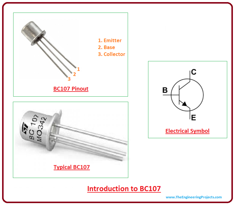
Introduction to BC107
- BC107 is an NPN bipolar planner low power transistor which is mainly designed for general purpose switching and amplification purpose.
- It is mainly composed of three terminals named as an emitter, base, and collector.
- Being a current controlled device, small current at the base side is used to control large current at the emitter and collector side.
- When a voltage is applied at the base terminal, it gets biased and draws current and starts controlling large current at the emitter and collector side.

- Movement of electrons plays an important role in the conductivity of any transistor. Bc107 is a bipolar junction transistor where conductivity is carried out by both charge carriers including electrons and holes but majority charge carriers are electrons.
- Free movement of electrons acts like a bridge between emitter and collector where emitter emits the electrons which are then collected by the collector.
- A base is used to control the number of electrons. As it is an NPN transistor so the base will be positive with respect to the emitter.
- Emitter, base, and collector are different in terms of their functions and doping concentrations.
- The emitter is highly doped as compared to base and collector. And voltage at the collector side is much larger than the base voltage.
- When two diodes are joined back to back, they constitute a bipolar junction transistor.
BC107 Pinout
Bc107 is an important device used for switching and amplification purpose. It consists of three terminals.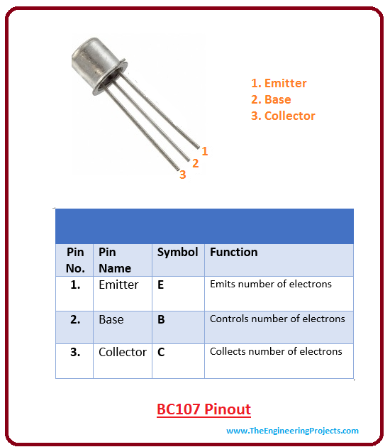
Circuit Diagram of BC107
Following figure shows the circuit diagram of bc107.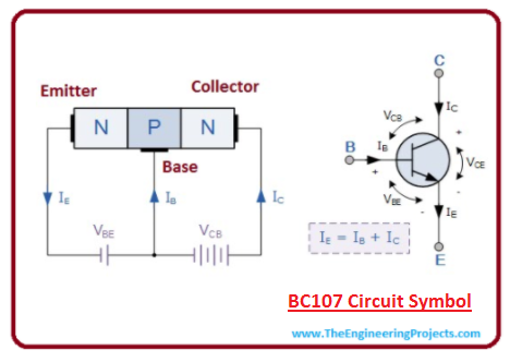
- Emitter current is equal to the sum of collector and base current.
- The ability of base current to control large emitter and the collector current is used for amplification purpose.
- This transistor is mainly used in three configuration common base configuration common collector configuration and common base configuration. Common emitter configuration is the basis of creating amplification because it shows exact voltage and current required for amplification purpose.
- Forward current is very helpful in defining the nature of amplification. It is also known as an amplification factor, or beta and denoted by ß.
- It is a ratio between collector current and base current and it exhibits no unit.
- Similarly, current gain is another important factor, also known as alpha, denoted by a and is a ratio between collector current and emitter current.
- The alpha value lies between 0.95 to 0.99 but most of the time its value is taken as unity.
Absolute Maximum Ratings
Absolute maximum rating of bc107 are shown in the figure below.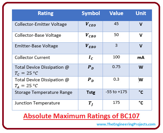
- Collector-Base and Collector-Emitter voltage are 50 and 45 respectively.
- Collector current is 100mA and maximum power it can dissipate at ambient temperature is 0.3 W.
- It is important to note that these are the stress ratings. If these stress ratings are increased from absolute maximum ratings, they can severely affect the quality of the device and ultimately damage it at large.
- Similarly, if stresses are applied for the extended period of time, they can affect the device reliability.
Difference between NPN and PNP Transistors
- NPN and PNP transistors are sometimes in same applications but there is a slight difference between them in terms of their functions and medium used for conductivity.
- Electrons are majority charge carriers in NPN transistors while holes are majority charge carriers in PNP transistors.
- Most of the professionals prefer NPN transistors over PNP transistor because conductivity carried out through electrons is better than conductivity carried out through holes.
Applications
- Signal Processing
- Power Management
- Portable Devices
- Consumer Electronics
- Industrial Purpose
×
![]()


