


Introduction to ATtiny85


Introduction to ATtiny85
- ATtiny85 is an 8-bit AVR microcontroller that comes with 8-pin interface and mainly used in automation and Arduino projects.
- The CPU is based on RISC architecture and is mainly called low power controller that stands fit for the real-time applications that can operate on minimum power.
- The program memory is 8KB while both EEPROM and RAM contain a memory space of around 512 bytes. These memory spaces are very useful for storing the number of instruction in the form of code.
- This module comes with only one port called Port B that is a bi-directional port and contains 6 I/O pins with internal pull-up resistors. The output buffers on PORTB are designed with symmetrical drive characteristics that come with both high sink and source capability. It is important to note that, Port B pins are externally pulled low and tri-stated that will source current if the pull-up resistors are activated.
- External and internal interrupts are available on the board, while 32 general purpose registers are included in the device that are mainly called data holding spaces.
- Two 8-bit timers are added in the device where one timer comes with compare modes and can be used both ways i.e. timer as well as a counter while other is high-speed timer/counter.
- This module comes with software select power saving modes that are very helpful for the applications that operate with minimum power.
- Like other controllers introduced by the Microchip, this module comes with 10-bit ADC converter that houses 4 analog channels that help in sensor interfacing and converting analog signals to digital ones.
- This tiny chip is available in four packages called PDIP, SOIC, TSSOP, and QFN where first three come with 8-pin interface while the last one contains 20 pins.
- Digital communications like I2C and SPI can be easily employed using this module that helps in developing a communication with external devices.
1. ATtiny85 Features
You have got a brief overview of this module. Now we cover the main features that will help you anticipate the major characteristic associated with the module. The following figure shows the complete features of ATtiny85.| ATtiny85 Features | |
|---|---|
| No. of Pins | 8 |
| CPU | RISC 8-Bit AVR |
| Operating Voltage | 1.8 to 5.5 V |
| Program Memory | 8K |
| Program Memory Type | Flash |
| RAM | 512 Bytes |
| EEPROM | 512 Bytes |
| ADC Number of ADC Channels | 10-Bit 4 |
| Comparator | 1 |
| Packages | PDIP (8-Pin) SOIC (8-Pin) TSSOP (8-Pin) QFN/MLF (20-Pin) |
| Oscillator | up to 20 MHz |
| Timer (2) | 8-Bit Timers |
| Enhanced Power on Reset | Yes |
| Power Up Timer | Yes |
| I/O Pins | 6 |
| Manufacturer | Microchip |
| SPI | Yes |
| I2C | Yes |
| Watchdog Timer | Yes |
| Brown out detect (BOD) | Yes |
| Reset | Yes |
| USI (Universal Serial Interface) | Yes |
| Minimum Operating Temperature | -40 C |
| Maximum Operating Temperature | 125 C |
- You must check these features before making a final decision to install and use this module for your relevant project.
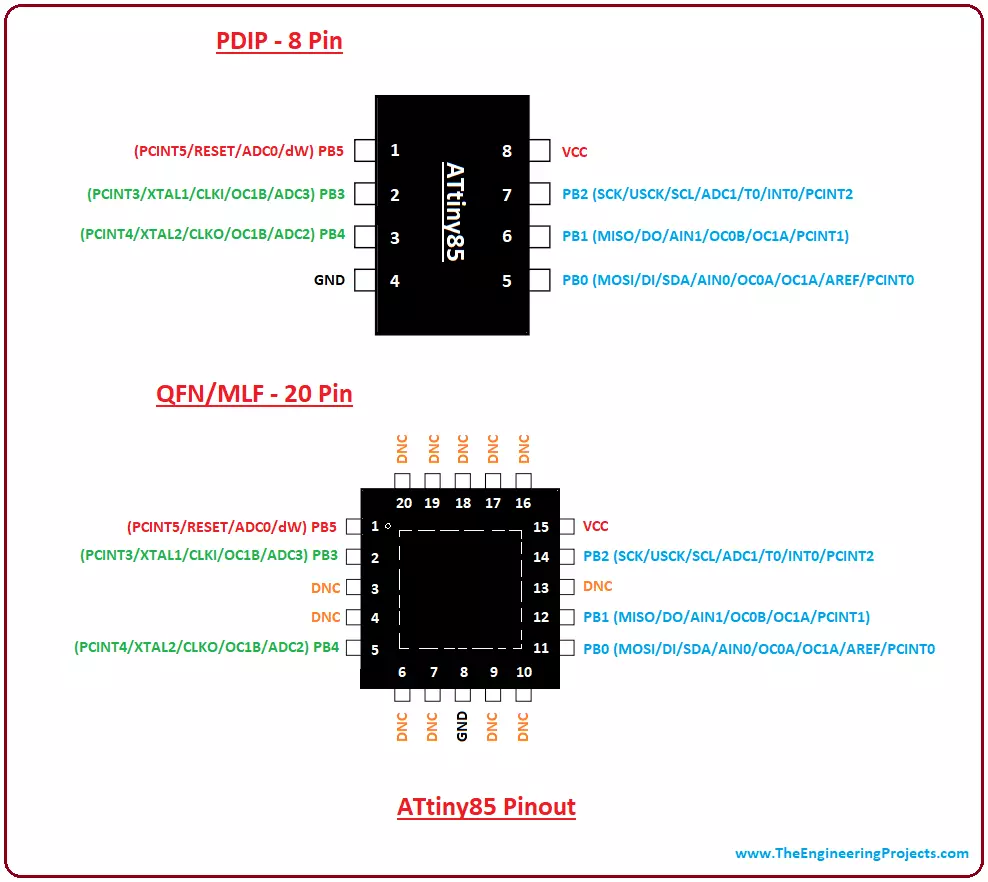
2. ATtin85 Pinout and Description
Until now, you have got a hold of basic information and complete features of ATtiny85. In this section, we will discuss the pinout and pin description of the module.Pinout
Following figure shows the pinout of ATtiny85.
- The bottom pad available on the board must be soldered to the ground.
- The DNC marked on the pinout stands for don't connect.
Pin Description
Following table shows the pin description that will help you understand the major functions associated with each pin.| Pin# | Pin Name | Pin Description |
|---|---|---|
| 1 | PB5 PCINT5 RESET ADC0 dW | I/O Bidirectional pin Interrupt Reset Analog Channel 0 Define Word |
| 2 | PB3 PCINT3 XTAL1 CLKI OC1B ADC3 | I/O Bidirectional pin Interrupt Crystal Oscillator Pin 1 Clock Analog Channel 3 |
| 3 | PB4 PCINT4 XTAL2 CLKO OC1B ADC2 | I/O Bidirectional pin Interrupt Crystal Oscillator Pin 2 Clock Analog Channel 2 |
| 5 | PB0 MOSI DI SDA AIN0 OC0A OC1A AREF PCINT0 | I/O Bidirectional pin SPI Serial Data (I2C) Analog Input Compare Register Voltage Reference Interrupt |
| 6 | PB1 MISO DO AIN1 OC0B OC1A PCINT1 | I/O Bidirectional pin SPI Serial Data (I2C) Analog Input Compare Register Interrupt |
| 7 | PB2 SCK USCK SCL ADC1 T0 PCINT2 | I/O Bidirectional pin Serial Clock Line (I2C) Analog Channel 1 Timer 0 Interrupt |
| 4 | GND | Ground Pin |
| 8 | Vcc | Voltage Supply Pin |
3. ATtiny85 Main Functions
ATtiny85 can perform a number of functions on a single chip. Some pins come with an ability to employ more than one functions. Following are the main functions of this module.Timers
There are two timers included on the chip that help in generating a delay in the running process of certain function when they work in a timer mode. In the counter mode, these timers are used to count the number of the interval on a specific function inside in the controller. The timer mode increments the instruction cycle while the counter mode is used to increment the rising and falling edge of the pin.SPI Communication
ATtiny85 comes with a serial peripheral interface (SPI) that is mainly used for communication between the microcontroller and other peripheral devices such as SD cards, sensors, and shift registers.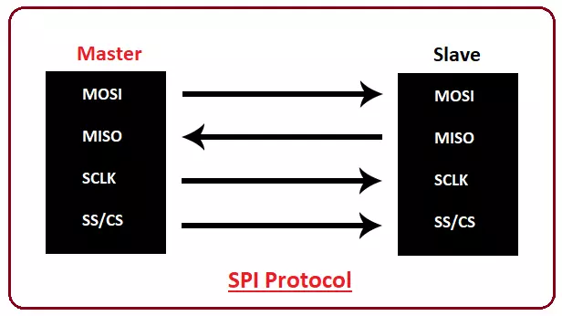
I2C Communication
I2C protocol is added in the device that is mainly two-wire protocol used to connect low-speed devices like ADC and DAC converters, I/O interfaces and microcontrollers. The two wires, known as Serial Clock (SCL) and Serial Data (SDA), are the main part of this communication protocol. The SCL line behaves like a clock signal that is generated by the master device and synchronizes the data transfer between the devices. While the SDA line is used to carry the required data.Brown Out Reset (BOD)
The BOD is a very useful function that helps in resetting the controller once the Vdd (voltage supply) drops below a brownout threshold voltage. The multiple voltage ranges are provided to secure the module once the power drops at the voltage supply line.Interrupt
The interrupt plays a vital role in an emergency which puts the main function on hold and executes the required instructions that are necessary at that time. Once the interrupt is executed the running code puts the controller back to the main program.ADC Converter
ADC module is a valuable addition in the device that makes it compatible with the sensors. It is a 10-bit module that contains 4 channels which are little less than the number of channels available on the modules introduced by Microchip that, more or less, come with 7 or 12 channels.4. ATtiny85 Memory Interface
The memory of this little toy is designed and based on Atmel's high-density technology that is basically non-volatile in nature. The Program Memory can be reprogrammed through SPI serial interface using two ways i.e. On-chip boot code or non-volatile memory programmer. The main program execution is mainly done inside CPU that plays a vital role to access memories and perform calculations on the basis of the number of instructions incorporated into the controller. This module falls under the category of AVR controllers that are based on Harvard architecture and come with separate locations reserved for both program and data memory.Program Memory (ROM)
Program memory, that is basically reprogrammable flash memory, works in a simple manner where next instruction stands in the queue once first is called and executed. This helps in executing the instructions with regular intervals in every clock cycle. The Flash memory comes with 8k memory space and contains memory endurance around 10,000 write/erase cycle (means you can erase and write the instructions 10,000 times on this board). The program counter available on the flash memory is 12bits wide that can address 4096 program memory locations.Data Memory (RAM)
The data memory comes with 512bytes memory space and reserves the memory locations three ways i.e. first 32 locations access the file register, next 64 locations are reserved for standard I/O memory and remaining are used for internal data SRAM. The data memory is categorized into five addressing modes named as- Direct,
- Indirect
- Indirect with Displacement
- Indirect with Pre-decrement
- Indirect with Post-increment
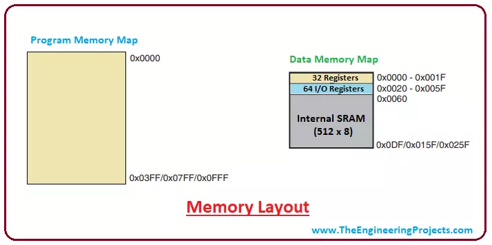
EEPROM Data Memory
This memory comes with 512 bytes of memory space which is designed and laid out as a separate data space where single bytes can be accessed. It comes with a memory endurance around 100,000 write/erase cycles which is ten times more than program memory.5. ATtiny85 Compilers
There are many compilers available for compiling the code in the AVR microcontroller. Some are better than others. Before you pick some compiler for your controller, make sure it is easy to use and stand fit for your needs and requirements.- If you are in the learning phase, then IAR is the best compiler for AVR. It is highly professional, though expensive, what it lacks in economical price, it covers up by providing both flawless quality and ease of use where it can support most, if not all, of the MCU families.
- ImageCraft is good option to start with that has made a decent place in the market but lack of GUI features make this compiler difficult to handle where editor and project management are quite daunting and can put you in a total stall in the start.
6. ATtiny85 Block Diagram
Block diagram is very helpful to visualize the main function available inside the controllers and how each feature and component are connected with each other. Following figure shows the block diagram of ATtiny85.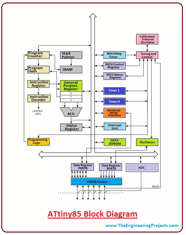
- The AVR core is used to combine 32 general purpose register with the rich instruction set.
- Also, these 32 registers are directly connected with the ALU (Arithmetic Logic Unit) which helps in accessing the two independent registers using single instruction.
7. Interfacing ATtiny85 with Arduino
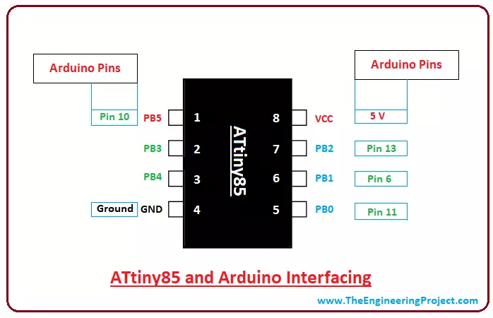
Tiny things can work wonders if used a proper way. Both ATtiny85 and Arduino, when connected, can easily drive automation in your project and help in executing the number of instructions. You can connect ATtiny85 with the Arduino following way.- Arduino Pin 10 ...................... ATtiny85 Pin 1
- Arduino Pin 11 ...................... ATtiny85 Pin 5
- Arduino Pin 12 ...................... ATtiny85 Pin 6
- Arduino Pin 13 ...................... ATtiny85 Pin 7
- Arduino +5V...................... ATtiny85 Pin 8
- Arduino Ground ...................... ATtiny85 Pin 4
- If you intend to work on this Arduino board then you must try these Arduino Projects for Beginners, they will anticipate how Arduino works.
8. Applications
- It is mainly used in real time applications related to industrial automation.
- Embedded Systems Projects make use of this module to drive automation.
- It can be employed and incorporated in robotics.
- Aeronautical technology houses a wide range of AVR controllers covering Quad-copter and space Aeroplanes.
- Power monitoring and management systems use this module.
×
![]()


