Introduction to 2n3055

Introduction to 2n3055
- The 2n3055 is a semiconductor NPN bipolar transistor which consists of three terminals called emitter, base, and collector.
- Unlike FETs(Field effect transistors) it is a current controlled device in which small current at the base side is used to control a large amount of current at the emitter and collector side.

- It is a bipolar device in which conduction is carried out by the movement of both charge carriers i.e electrons and holes.
- The measure of base current to control the large current at the emitter and collector side is used for amplification purpose.
- As 2n3055 is an NPN transistor, here base with positive with respect to emitter and P layer lies between the two layers of N doped semiconductor.
- P-doped layer of transistor acts like a base while other two N sides represent emitter and collector respectively.
- It comes with lots of electronic applications but mostly it is used for switching and amplification purpose.
- This NPN transistor can be configured with three configurations named as a common collector, common base, and common emitter configuration.
- It is important to note that it won't be useful for amplification purpose when it is configured with common emitter configuration as it encompasses a transition frequency of around 3 MHz that will allow the forward current gain drop to 1.
- The maximum collector-emitter voltage is highly dependent on the resistance intensity between emitter and base, provided by the external circuit.
- The 2n3055 is connected to a heat sink which widely effects the overall power dissipation by the transistor.
- However, in most of the application when an ambient temperature is high, low power dissipation is expected.
- This device is manufactured in such a way it can function with an efficient heat sink.
- However, proper care should be given in order to mount the device perfectly, otherwise, it can harm the device at large.
- Mica insulator is added in the manufacturing process that isolates the case of the transistor from the heat sink.
- This transistor is a bipolar current controlled device which is different than JFET which is a unipolar voltage controlled device.
2n3055 Pinout
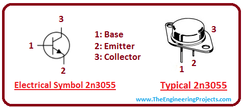
2n3055 consists of three terminals which are given below. 1: Emitter 2: Base 3: Collector Pinout of 2n3055 is given in the figure below.
- A small amount of base current is used to control the large current at the emitter and base side.
- Conduction is carried out when electrons emit from the emitter and are collected by the collector.
Circuit Diagram of 2n3055
The circuit symbol of 2n3055 is shown in the figure given below.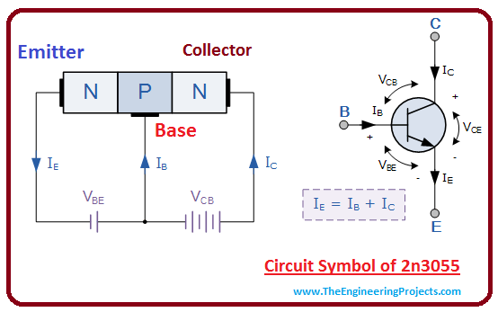
- As it is an NPN silicon transistor so it has positive base terminal and a negative emitter terminal.
- This transistor is a current controlled device where a small amount of current at the base side is used to handle a large amount of current at the emitter and collector side.
- The NPN and PNP transistor encompass same features with some exceptions i.e. Current will sink into the base side in case of PNP transistor while current from the base side will source to the transistor in case of NPN transistor.
- Emitter current is the sum of base and collector current.
- Transistor forward current gain can be found by dividing the collector current to the base current. It is also called beta current and is denoted by ß. Beta has no units as it is a ratio between two currents.
- Beta value is used for the amplification purpose. Beta value ranges between 20 to 1000, however, its standard value is 200.
- At positive base to collector voltage, the ratio between collector current to the emitter current is called current gain of the transistor and is denoted by alpha a.
- The value of alpha lies between 0.95 to 0.99, however, in most of the cases it is considered as 1.
Maximum Rating of 2n3055
Absolute maximum rating of 2n3055 are given below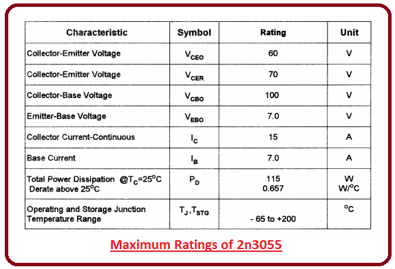
- It dissipates power around 115 W when the case temperature is set to 25 degrees.
- It is a 60 V and 15 A device which comes with a base current of 7 A and forward current gain ranges between 20 to 70.
Applications
- It is widely used in lots of applications where amplification of the signal is required.
- It is used for switching purpose.
×
![]()


