Introduction to BC182L

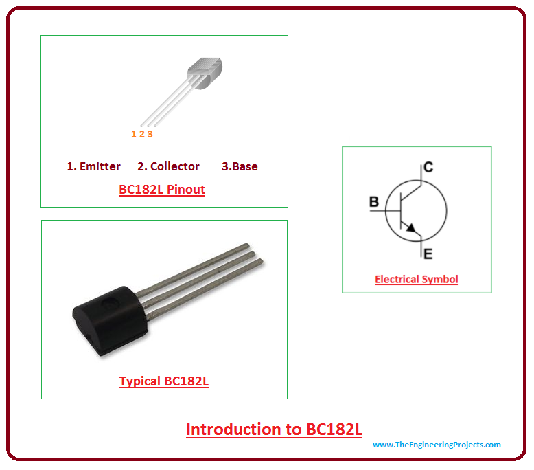
Introduction to BC182L
- BC182L is an NPN bipolar general purpose transistor which is mainly used for switching and amplification purpose at a collector current to 100mA.
- It is a bipolar transistor, means conduction is carried out by the movements of both charge carriers i.e electrons and holes, however, majority charge carriers are electrons.
- It consists of three terminals called emitter, base, and collector. Each terminal comes with a specific function associated with it.
- BC182L is an NPN transistor, where a base is positive with respect to emitter and voltage at the collector side is more than base. Emitter, base, and collector are different in terms of size and doping concentration.

- An emitter is highly doped as compared to collector and base, while a base is lightly doped.
- It is a current controlled device where small current at the base side is used to control large current at the emitter and collector side.
- When a voltage is applied at the base terminal, it gets biased and draws current which is used to control large current at the other terminals.
- The emitter emits the electrons which are then collected by the collector; the base is mainly used for controlling the number of electrons.
- Actually, free movement of electrons acts like a bridge between emitter and collector.
- Transistor is nothing but a combination of diodes joined back to back.
BC182L Pinout
BC182L mainly consists of three terminals. 1. Emitter 2. Collector 3. Base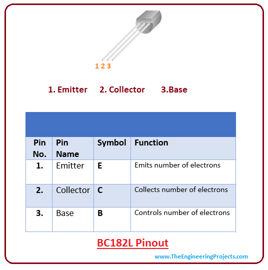
- Movement of electrons plays an important role in the conductivity of the transistor.
- And electron reaction starts when a voltage is applied at the base terminal.
Circuit Diagram of BC182L
Following figure shows the circuit diagram of the BC182L.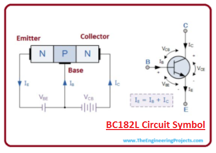
- We can see from the figure, emitter current is equal to the sum of base and collector current. Because emitter is bigger than collector and base in terms of doping concentration.
- BC182L is an NPN transistor and it will source the base current to the transistor.
- The measure of a number of electrons that pass from base to collector is called transistor efficiency.
- The base is lightly doped and an emitter is heavily doped that will allow the electron to move from the emitter to base more than it will allow the holes from base to emitter.
- Forward current gain plays an important role for amplification purpose. It is called beta, denoted by ß, and it is a ratio between collector current and base current. Beta value ranges between 20 to 1000, however, it has standard value 200.
- Current gain is another important factor which is called alpha, denoted by a, and it is a ratio between collector current and emitter current. Alpha value ranges between 0.95 to 0.99 however, most of the time alpha value is considered as a unity.
- Almost all the transistors operate in forward biased mode. If we interchange emitter and collector and makes them reverse biased, then the value of alpha and beta will be much lesser than they will be in forward biased mode.
- This NPN transistor comes with electrons as major charge carriers while PNP transistor comes with holes as majority charge carriers.
Absolute Maximum Ratings
Following figure shows the absolute maximum ratings of this component.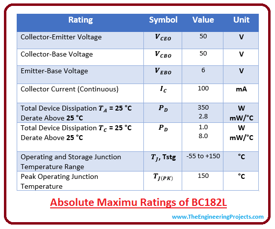
- These are the stress ratings, which if exceeded from the absolute maximum ratings, can damage the device severely and affect the overall quality of the component.
- If these stresses are applied for the extended period of time, they can affect the reliability of the device.
- In order to avoid any loss or damage, it is recommended to follow the operating conditions given by the manufacturer. Taking measures and following proper protocols in the early stage of your project can save you both cost and time.
- I'd suggest you have a look at 2n3903 if you require different ratings as compared to this transistor.
Applications
- It is mainly used for amplification and switching purpose.
- Audio and signal processing makes use of this transistor.
×
![]()


