74LS238 Datasheet, Pinout, Features, Working and Simulation


Hey readers! I hope you are doing great. Welcome to another article where we are discussing the integrated circuit device. Today, we’ll study the 74LS238 IC, which is a widely used component in different digital circuits as a multiplexer and demultiplexer. Multiple features of this IC, such as its low power performance and versatility, make it a good choice for electronic circuits.
In this article, you will see the basic introduction of 74LS238, the datasheet of this IC, its working principle, the simulation in Proteus, and its applications in detail. There is a lot of information to understand about this 3 to 8 line decoder and we’ll shed light on all these topics from scratch so let’s start working on it.

Figure 1: Basic structure of 74LS238 IC
74LS238 Introduction
- The 74LS238 is an integrated circuit that belongs to the transistor-transistor logic (TTL) family and is part of the Shcottkey series.
- It is a 16-pin DIP IC and the LS in the name of this decoder indicates low-power performance.
- It is a 3 to 8 line decoder and demultiplexer and generally, the following points are covered in its working:
It is designed to take three inputs in binary format only
The internal structure of this IC performs complex calculations of demultiplexing or decoding according to the circuit
On the output side, the inputs are converted into eight mutually exclusive outputs and the high value is only at one output
This IC is widely used in different digital circuits because of its versatility.
It has a reliable, simple, and straightforward working nature. Moreover, it is also preferred to convert complex circuits into simple ones because of their fine structure and the ability to fit in multiple types of circuits.
It has the feature of minimizing the effect of system decoding.
74LS238 Datasheet
The details of the structure and functionalities of the 74LS238 IC can be understood from the details of its datasheet. Here are different points about this IC:
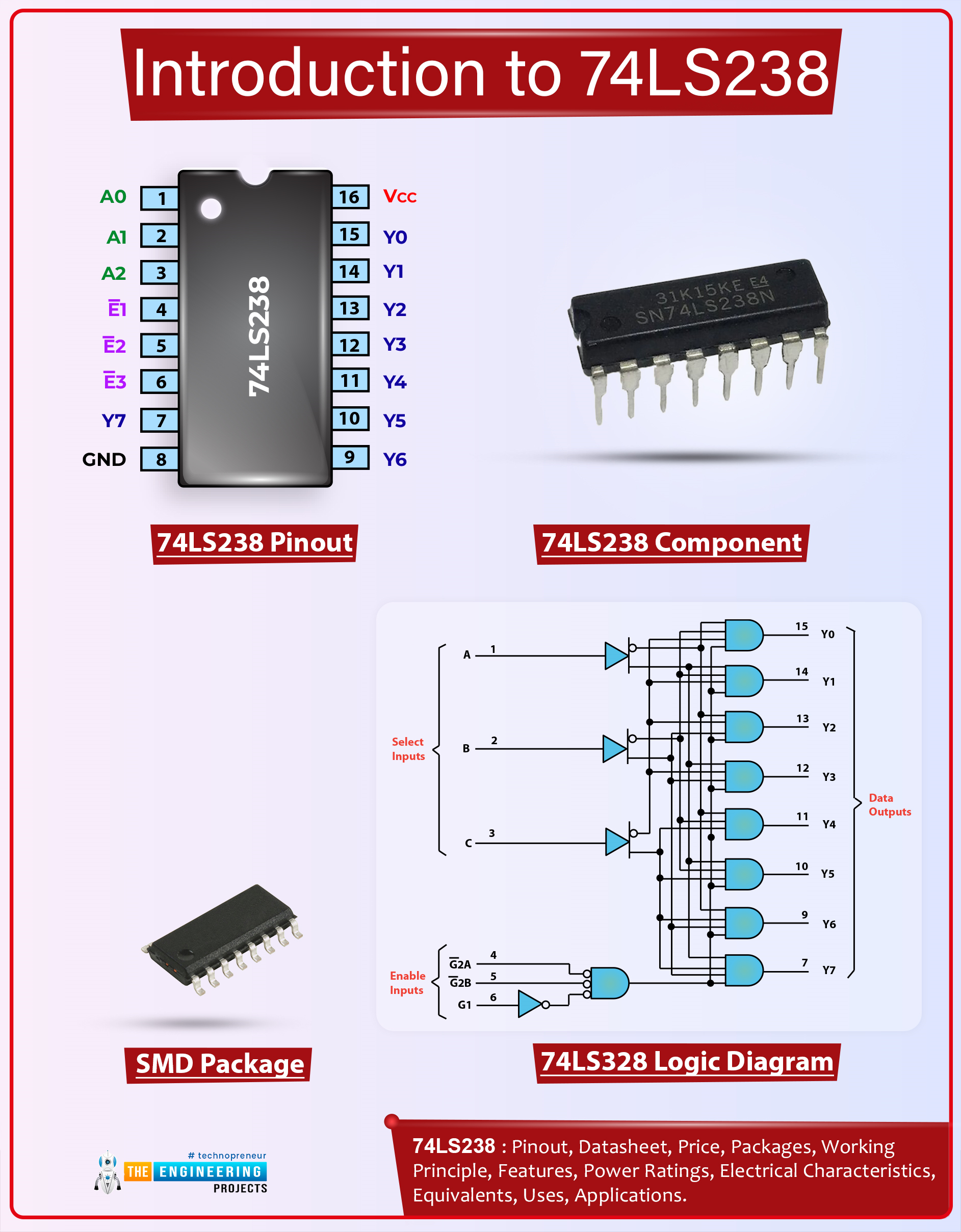
74LS238 Pinout Configuration
This IC has 16 pins that are packed in the dual inline package (DIP). Here is the diagram that describes its structure:

Figure 2: Pinout configuration of 74LS238
All the pin numbers have a specific name in alphanumeric format. The details of each pin and its description are given here:
Symbol |
Pin Number |
Description |
Active State |
A0 |
1 |
Address input |
- |
A1 |
2 |
Address input |
- |
A2 |
3 |
Address input |
- |
E1 |
4 |
Enable input |
LOW |
E2 |
5 |
Enable input |
LOW |
E3 |
6 |
Enable input |
HIGH |
Y0 |
7 |
Output |
HIGH |
Y1 |
9 |
Output |
HIGH |
Y2 |
10 |
Output |
HIGH |
Y3 |
11 |
Output |
HIGH |
Y4 |
12 |
Output |
HIGH |
Y5 |
13 |
Output |
HIGH |
Y6 |
14 |
Output |
HIGH |
Y7 |
15 |
Output |
HIGH |
GND |
8 |
Ground (0 V) |
- |
VCC |
16 |
Supply voltage |
- |
Table 1: Pinout configuration of 74LS238
74LS238 Function Table
The 74LS238 is used as the 3 to 8 line decoder. The binary combination of three inputs results in different outputs. Here is the detail in the form of the function table:
Enable Inputs |
Select Input |
Outputs |
|||||||||||
G1 |
G2A |
G2B |
C |
B |
A |
Y0 |
Y1 |
Y2 |
Y3 |
Y4 |
Y5 |
Y6 |
Y7 |
X |
H |
X |
X |
X |
X |
L |
L |
L |
L |
L |
L |
L |
L |
X |
X |
H |
X |
X |
X |
L |
L |
L |
L |
L |
L |
L |
L |
L |
X |
X |
X |
X |
X |
L |
L |
L |
L |
L |
L |
L |
L |
H |
L |
L |
L |
L |
L |
H |
L |
L |
L |
L |
L |
L |
L |
H |
L |
L |
L |
L |
H |
L |
H |
L |
L |
L |
L |
L |
L |
H |
L |
L |
L |
H |
L |
L |
L |
H |
L |
L |
L |
L |
L |
H |
L |
L |
L |
H |
H |
L |
L |
L |
H |
L |
L |
L |
L |
H |
L |
L |
H |
L |
L |
L |
L |
L |
L |
H |
L |
L |
L |
H |
L |
L |
H |
L |
H |
L |
L |
L |
L |
L |
H |
L |
L |
H |
L |
L |
H |
H |
L |
L |
L |
L |
L |
L |
L |
H |
L |
H |
L |
L |
H |
H |
H |
L |
L |
L |
L |
L |
L |
L |
H |
Table 2: Function table of 74LS238
74LS238 Alternatives
The following are some other devices that have similar features and can be used in place of 74LS238:
74HC238
SN74HCT238
LS238C
TS74HC238P
74LS328 Logic Diagram
We know that ICs are made of a combination of logic circuits. The internal structure of these ICs makes the concept of working of the IC clear. If you want to have the details of its structure, you can have a look at the logic diagram of 74LS238 in a positive state:

Figure 3: Logic diagram of 74LS238
If you want to learn this datasheet in detail, you can have a look at the linked article give here:
74LS328 Working Principle
The basics of the working of this IC in detail are shared with you so that you may know the expected outcomes when using the 74LS238:
74LS238 Input Combination
This IC consists of three inputs that take only binary information. It means the inputs are only in the form of 0 and 1. The combination of these numbers decodes the output line, where the signals will be high.
74LS238 Decoding Logic
The decoding logic of the 74LS238 depends on the internal structure that varies from manufacturer to manufacturer. The logic diagram is shared with you in this tutorial. Different combinations of these logic gates are used to get the required output.
This IC usually consists of AND and NOT gates that process the inputs together and provide the expected output at the output.
74LS238 Output Selection
The internal structure is responsible for setting one of the eight bits high. This is the basic expectation of this integrated circuit. After processing the input bits, only one output bit is selected where the HIGH signals are sent. All other bits remain low.
74LS238 Enable Control
There are three enable pins (E1, E2, and E3) that work as the master switch of the decoder. The functionality of each of these is given next:
The E1 and E2 pins work closely with each other and if any one of these is HIGH, the output is always HIGH, no matter what the inputs are.
The pin E3 provides additional control over the output of the decoder. It is an important pin because it acts as the AND gate with three inputs and the overall output is HIGH only when the result of this AND gate combination is set to LOW.
74LS238 Simulation in Proteus
If you want to check the working of this IC then a good option is the proteus simulation. Here, I have created a simple circuit of this IC that will help you understand how the output is generated with 74LS238:
Material Required
74LS238 Features and Specifications
Till now, I hope you have an idea of the working of this IC but I have created a table that clearly describes its features and specifications of 74LS238 at a glance:
Category |
Feature |
Description |
General Information |
Function |
3-to-8 line decoder with active LOW outputs |
Family |
TTL (Transistor-Transistor Logic) |
|
Logic Level |
Low-power Schottky (LS) |
|
Package Type |
DIP (Dual In-Line Package) with 16 pins |
|
Inputs |
A0, A1, A2 |
Binary address inputs (3 lines) |
E1, E2, E3 |
Enable inputs (3 lines, all must be LOW to enable outputs) |
|
Outputs |
Y0 to Y7 |
Active LOW decoded outputs (8 lines) |
Key Specifications |
Propagation Delay |
15 ns typical |
Power Dissipation |
19 mW typical |
|
Supply Voltage |
4.75 V to 5.25 V |
|
Operating Temperature |
0°C to 70°C |
74LS238 Physical Dimensions
Before designing the circuit with the 74LS328, it is crucial to know the dimensions of this IC. Here is the table that describes its exact size in metric and imperial units:
Dimension |
Value (mm) |
Value (inches) |
Width |
6.10 |
0.240 |
Length |
9.91 |
0.390 |
Height |
3.81 |
0.150 |
Lead Spacing |
2.54 |
0.100 |
74LS238 Applications
The 3 to 8 line decoders have applications in multiple fields where the digital circuits are the basic devices. The main application of 74LS238 is in the form of a 3 to 8 line decoder and here are some examples of its applications:
74LS238 for Memory Address Decoding
In circuits like memory banks, an important process is to calculate the higher address bit. Here, the 74LS238 is widely used and its basic duty is to activate the most appropriate memory chip. In some cases, it also activates the specific memory location within that chip.
74LS238 in Microprocessors
Some microcontrollers have limited input-output ports, therefore, ICs like 74LS238 are used to expand the availability of the pins by providing the decoding process. Through decoding, the microprocessor can successfully select the required device at a time.

74LS238 in the Display Control
In display devices where the output is created by stimulating the specific arrangement of the LEDs, the 74LS238 plays a crucial role. For instance, in the 7-segment display, 74LS238 can illuminate the particular segments. As a result, the output shows the particular digit.
74LS238 in the Simplification of Circuits
The logic circuits consist of multiple logic gates and other related components. Logic gates are simple circuits and provide basic functionality but if the user wants to have a higher level of performance, there is a need for complex circuitry that is difficult to understand. The 74LS238 has built-in decoding functionalities therefore, using this IC in the logic circuit is a good idea to reduce the complexities of the circuit.
In this way, we have understood the basic information of the 74LS238 in detail. In this article, we have started from the scratch and learned about the introduction of the 74LS238 in detail. We saw the datasheet of this IC and understood the basic features in detail. We also created the simulation of 74LS238 in Porteus and in the end, we saw the physical dimensions and applications of this decoder. I hope this was a useful study for you and if you want to add more authentic information to it, you can contact us.