MJE13003 NPN Transistor Datasheet, Pinout, Features & Applications


Introduction to MJE13003
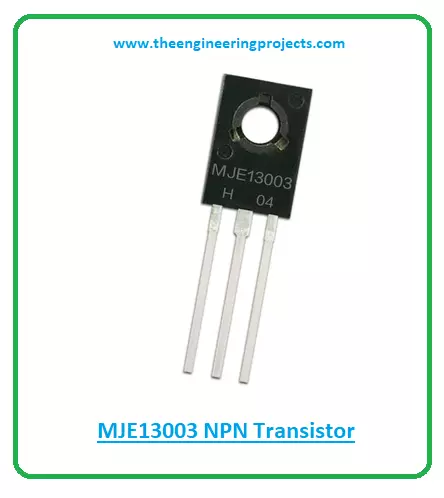
- MJE13003 is a bipolar junction transistor that belongs to the NPN transistor family. It is mainly used for switching and amplification purposes and comes in the TO-220 package.
- The power dissipation of this device is 40W which is the amount of power released during the working of this device.
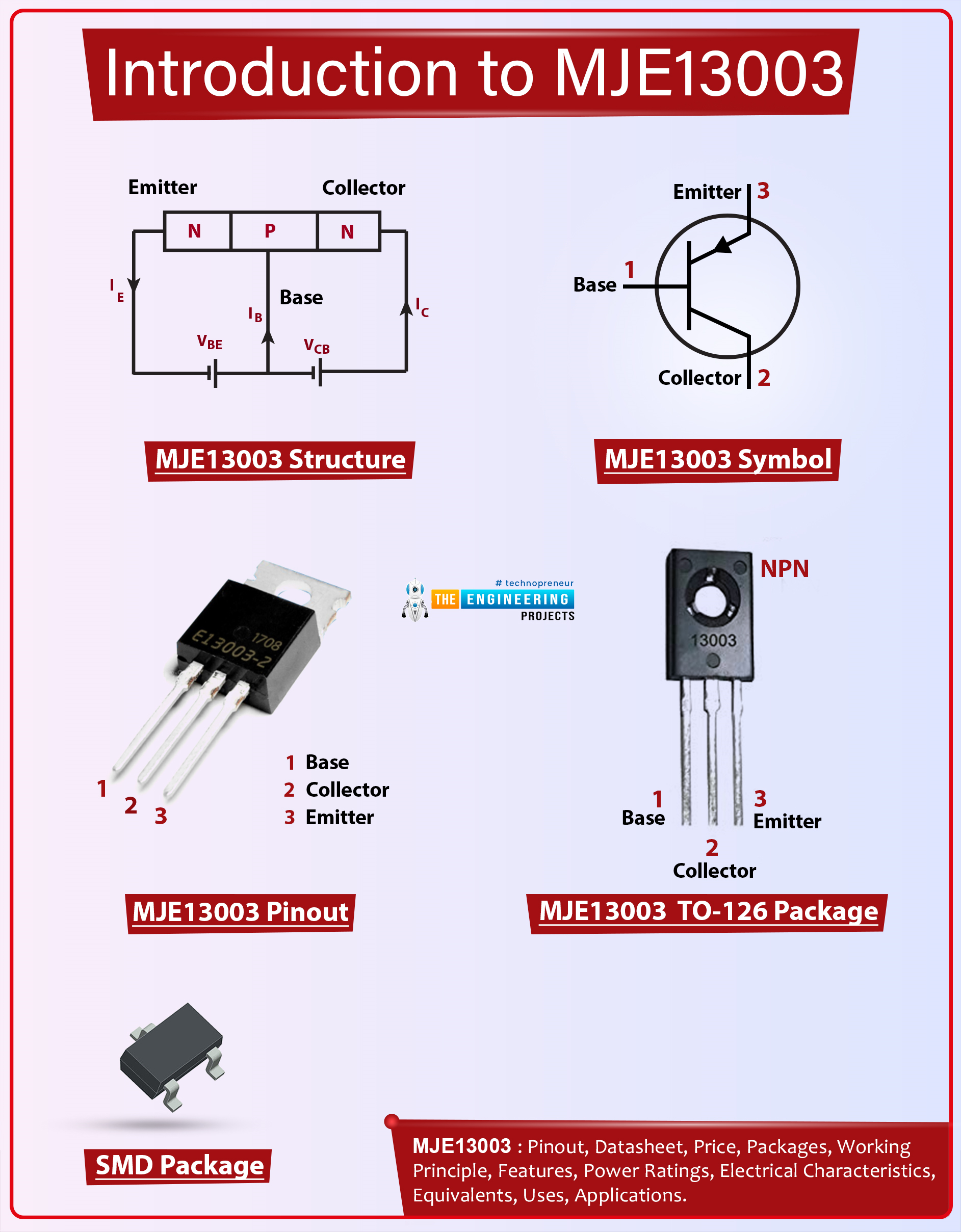
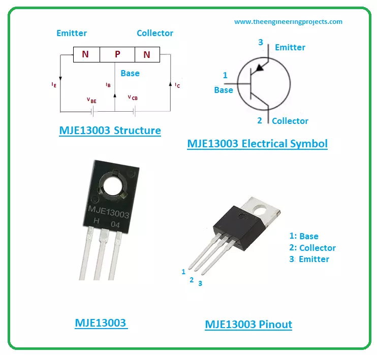
- MJE13003 is a power transistor that comes with three terminals known as emitter, base, and collector. The small input current at the base pin is used to induce a large output current at the emitter and collector terminals.
- Bipolar junction transistors are the type of transistors where two charge carriers i.e. holes and electrons, play a vital role in the conductivity of the device.
- Bipolar junction transistors are divided into two types where one is an NPN transistor and the other is a PNP transistor.
- In NPN transistors, both electrons and holes are responsible for the conductivity of the device, however, electrons are major charge carriers in this case while holes are minority carriers.
- Similarly, both electrons and holes play a vital role in the conductivity of PNP transistors but here holes are majority carriers and electrons are minority carriers.
- Moreover, current flows from emitter to collector terminal in PNP transistors while in the case of NPN transistors current flows in opposite direction i.e. from collector to emitter terminals.
- When comparing NPN transistors with PNP transistors, the NPN transistors are preferred over PNP transistors because electrons can flow faster than holes, making PNP devices more valuable for a range of applications.
- These bipolar junction transistors are current-controlled devices while MOSFETs are the type of transistors that are voltage-controlled devices and carry terminals named drain, source, and gate.
MJE13003 Datasheet
It is wise to scan through the datasheet of the component before you incorporate this device into your electrical project. The datasheet features the main characteristics of the device. You can download the datasheet of MJE13003 by clicking the link below.MJE13003 Pinout
MJE13003 is a power transistor that comes with three terminals named:- Base
- Collector
- Emitter
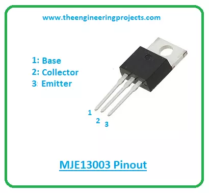
- The external electrical circuit is connected with this transistor through these terminals. All these terminals come with different doping concentrations.
- The emitter pin is highly doped while the collector pin is lightly doped. And the base terminal is 10-times more doped than the collector pin.
- And large current at the emitter and collector terminals is produced by using the small current at the base terminal.
MJE13003 Working Principle
- The base pin is the location responsible for the entire transistor action. When you apply a voltage at the base pin, it will bias the device and as a result, the current will start flowing from collector to emitter terminal.
- As this is an NPN transistor so here electrons are the major carriers and holes are minority carriers.
- Know that bipolar junction transistors are not symmetrical devices. Which projects if you interchange the emitter and collector terminal, it will prevent the terminals to work in forward active mode, and thus both terminals will start working in reverse active mode.
- Exchanging these terminals will also influence the values of common-base current gain and common-emitter current gain.
MJE13003 Absolute Maximum Ratings
The following table shows the absolute maximum ratings of MJE13003.| Absolute Maximum Ratings of MJE13003 | ||||
|---|---|---|---|---|
| Pin No. | Pin Description | Pin Name | ||
| 1 | Collector-emitter voltage | 400V | ||
| 2 | Collector-base voltage | 700V | ||
| 3 | Base-emitter voltage | 9V | ||
| 4 | Collector current | 1.5A | ||
| 5 | Power dissipation | 40W | ||
| 6 | Base current | 0.75A | ||
| 7 | Operating and storage junction temperature range | -55 to 150C | ||
- The total power dissipation of this device is 40W which is the amount of power released during the functioning of this device.
- While collector-base voltage is 700V and collector-emitter voltage is 400V. The emitter-base voltage is 9V which shows the amount of voltage required to bias this device.
- When you’re working with the component, make sure the ratings don’t surpass the absolute maximum ratings. Otherwise, they can badly damage the device, thus the entire project.
- Also, don’t apply these ratings more than the required time, else they can affect device reliability.
MJE13003 Applications
MJE13003 is employed in the following applications.- Used in modern electronic circuits.
- Used in the switched-mode power supply.
- Used in voltage regulator circuits.
- Used for switching and amplification purpose.
- Used in Bistable and Astable multivibrators circuit.
- Used to support loads under 1.5A.
- Used in H-bridge circuits.
- Used in the motor control circuit.
MJE13003 Physical Dimensions
The following figure shows the physical dimensions of MJE13003.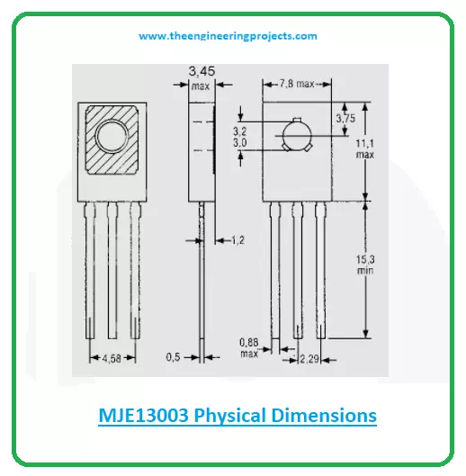
×
![]()