Hello Learners! Welcome to The Engineering Projects. In the previous tutorial, we discussed the first universal gate i.e. NOR Gate and simulated it in Proteus. Today, we are going to focus on the second universal gate i.e. NAND Gate. We will also derive basic logic gates from the NAND gate, to prove its universality.
Today, we'll seek the answers to the following questions:
What is a NAND Gate?
What is a Universal Gate?
NAND as a Universal Gate.
NAND Gate as Universal Gate in Proteus ISIS.
Let's get started:
What is a NAND Gate?
A NAND Gate is designed by inverting the output of AND Gate and thus it gives a LOW output when all of its inputs are HIGH, otherwise, it's HGIH.
In order to design a NAND gate, simply place a NOT gate in front of the AND gate.
A and B are two inputs of the NAND Gate, Output Y is denoted by a dot between the inputs along with a combined compliment or a bar on the whole statement.
Y= (A.B)'
The graphical symbol of the NAND Gate is the same as that of the AND gate, except there's a small bubble at the start of the output to represent NOT. The graphical representation of the NAND gate is shown in the below figure:
Truth Table and Timing Diagram of NAND Gate
Here's the Truth Table of the NAND Gate(Inverse of AND Gate):
A
B
(A.B)’
0
0
1
0
1
0
1
0
0
1
1
0
The timing diagram of the NAND gate is shown below:
What is a Universal Gate?
In Logic Circuits, we often use a term called "Universal gates". this can be defined as:
"The category of Logic Gates, through which we can derive all the Basic Gates are called universal Gates."
We have two Universal Gates, NAND Gate and NOR Gate. These have importance in the world of Digital Logic Designs because of their simplicity and usefulness.
NAND as a Universal Gate
As discussed before, NAND Gate is a Universal Gate because we can design any logic gate with a NAND Gate. Let's design the following logic gates with a NAND Gate:
OR Gate
AND Gate
NOT Gate
Components Required:
NAND Gate
Logic Toggle
Logic Probe
Connecting Wires
Take the discussed elements from the pick library One after the other through "P" button.
Follow the instructions to make all the Gates one by one.
Basic Gates through NAND Gate
OR Gate
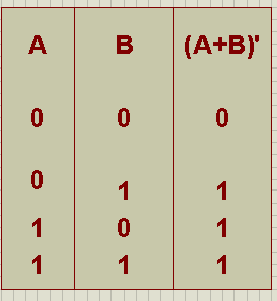
While Designing the OR Gate through NOR Gate, we must have the knowledge about one rule of Digital Logic Design that says:
"The Compliment of the ANDed input is equal to the ORed inputs."
Mathematically,
(A'B')'=A+B
Take an NAND gate from the library and fix it at the working area.
Repeat the step two times.
Connect the output of two NAND Gates with the input of third one.
Connect the inputs of other two remaining Gate with each other through a wire to set them as one input.
Connect logic Toggles as the input with two NAND Gates.
Join Logic Probe to visualize the output.
The circuit looks like this:
Pop the play button.
Change the value of inputs one by one and record the output in the form of table.
AND Gate
We'll Design AND Gate through NAND Gate on the basis of the following rule of logic Design:
"The Compliment of ANDed inputs is equal to the ANDed inputs."
(A.B)'=A.B
Get two NAND Gates from Pick Library.
Set them at the working area.
Join then inputs of 2nd Gate with each other.
Set Logic toggles at the input of the 1st one.
Join Logic Probe with the output of 2nd one.
Connect the output of the 1st Gate with the inputs of the other.
Change the inputs through Logic Gates.
Record the truth table according to the output.
NOT Gate
The formation of NOT Gate through NAND Gate is based upon the rule:
"The Compliment ANDed input with itself is equal to the complement of input."
(A.A)'=A'
Take the NAND Gate.
Fix it at working area.
Connect its both inputs with each other.
Connect Logic Toggle and Logic Probe.
Change the inputs.
The resultant Truth Table is:
NOTE: You can Gain the same output by following the rule (A.1)'=A'
Advantages of NAND Gate
NAND Gate is a universal gate therefore it can make the circuit less complex.
We can use them for the functionality of more than one Gate.
It stores more storage capacity as compared to its size.
It is Cost effective per byte.
Real life Applications of NAND Gate
Freezer warning buzzers.
Burglar Alarms.
Disadvantages of NAND Gate
It is Difficult to design than other Gates.
It has propagation delay.
The high Gate count is also a disadvantage.
Consequently, we recognized the Core detail of NAND gate, we learnt what are the universal gate and how can we make different gates with NAND gate using Proteus simulation. moreover, we got some of the advantages, disadvantage and some real life applications of NAND Gate.