What are DLD Logic Gates? Symbol | Truth Table | Simulation


Hello Mentees! I hope you all are doing well. In today's article, we'll learn about the very basic pillar of Digital Logic Circuits i.e. Logic Gates. As we know, the digital world depends on Boolean digits either 0 or 1. So, there's always a need to perform different operations on these boolean numbers i.e. addition, subtraction, multiplication, shifting etc. In order to perform these operations on the binary signals, we use Digital Logic Gates in DLD circuits.
So, let's have a look at What is a Logic Gate:
What is a Logic Gate?
- Logic Gates are designed to perform a specified operation(i.e. addition, bit shift etc.) on the input signals and generate the output signal.
- For example, a simple NOT gate takes a single binary input and returns its inverse in the output, i.e.
- If Input is 0, the Output will be 1.
- If Input is 1, the Output will be 0.
- We can design Logic gates using basic electronic components i.e. resistor, diode, transistor, etc. However, in order to design gates for commercial use, two main manufacturing technologies are used, i.e:
- TTL(Transistor-Transistor Logic): TTL Logic gates use NPN & PNP Bipolar Junction Transistors in their circuitry i.e. 7400 series.
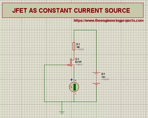
- CMOS(Complementary Metal Oxide Silicon): CMOS Logic Gates use MOSFET or JFET transistors(i.e. 4000 series)yea ri and are quite popular because of their ultra-quick response.
Symbolic Representation
- Each Logic gate is assigned a symbol for its representation, which simplifies the designing of their circuit diagrams.
- The symbolic representation of 4 basic logic gates is as follows:

Truth Table
- Every logic gate has a truth table(also called a logical table), used to provide the output states for all the possible combinations/conditions of its inputs.
- It's a convention to write the outputs in the right-side columns and the inputs in the left-side columns.
- The truth table of NOT Gate(used to inverse input), is shown in the below figure:
| Input |
Output |
| 0 | 1 |
| 1 |
0 |
- As you can see in the above figure, the table has 2 rows in total giving us all the possible input conditions.
- The number of rows in a truth table depends on the number of inputs used. The formula is, if we have "n" number of inputs in a logic gate, its truth table will have 2n rows in total. So, if we have 2 inputs, the rows of its truth table will be 22 = 4.
Truth tables are useful in Boolean and mathematical operations as the relationship between the Input and Output can be understood at a glance.
Now let's have a look at the Circuit Designing of Logic Gates:
Logic Gates Circuit Designing
As we discussed earlier, different Manufacturing Techniques are used to design logic gates. These techniques decide the characteristics of the logic gates i.e.
response time, noise immunity, voltage level for logic shifting etc. We can use simple electronic components i.e. diode, transistor, resistor etc. to design logic gates. The normal practices for designing logic gates with simple electronic components are:
- RTL (Resistor-Transistor Logic)
- DTL ( Diode-Transistor Logic)
- ECL (Emitter-Coupled Logic)
- DRL (Diode-Resistor Logic)
Such logic gates are quite simple in designing and normally have quite low response time and may also provide false output because of noise. So, in order to overcome these issues, these two manufacturing techniques are used:
- TTL(Transistor-Transistor logic)
- CMOS(Complimentary Metal oxide Semiconductors)
Simple NPN and PNP transistors are used in TTL logic gates and thus have better response time as compared to basic logic gates. In the CMOS technique, MOSFET and FET are used to control the logic and thus provide the best response time and are quite immune to noise. So, among all these manufacturing techniques, CMOS is considered the most popular technique for logic gate designing.
Logic Gates Designing with Basic Components
Here is an example of an AND Gate design with a Diode-Resistor Logic(DRL) and a NAND gate designed with Diode-Transistor Logic (DTL):
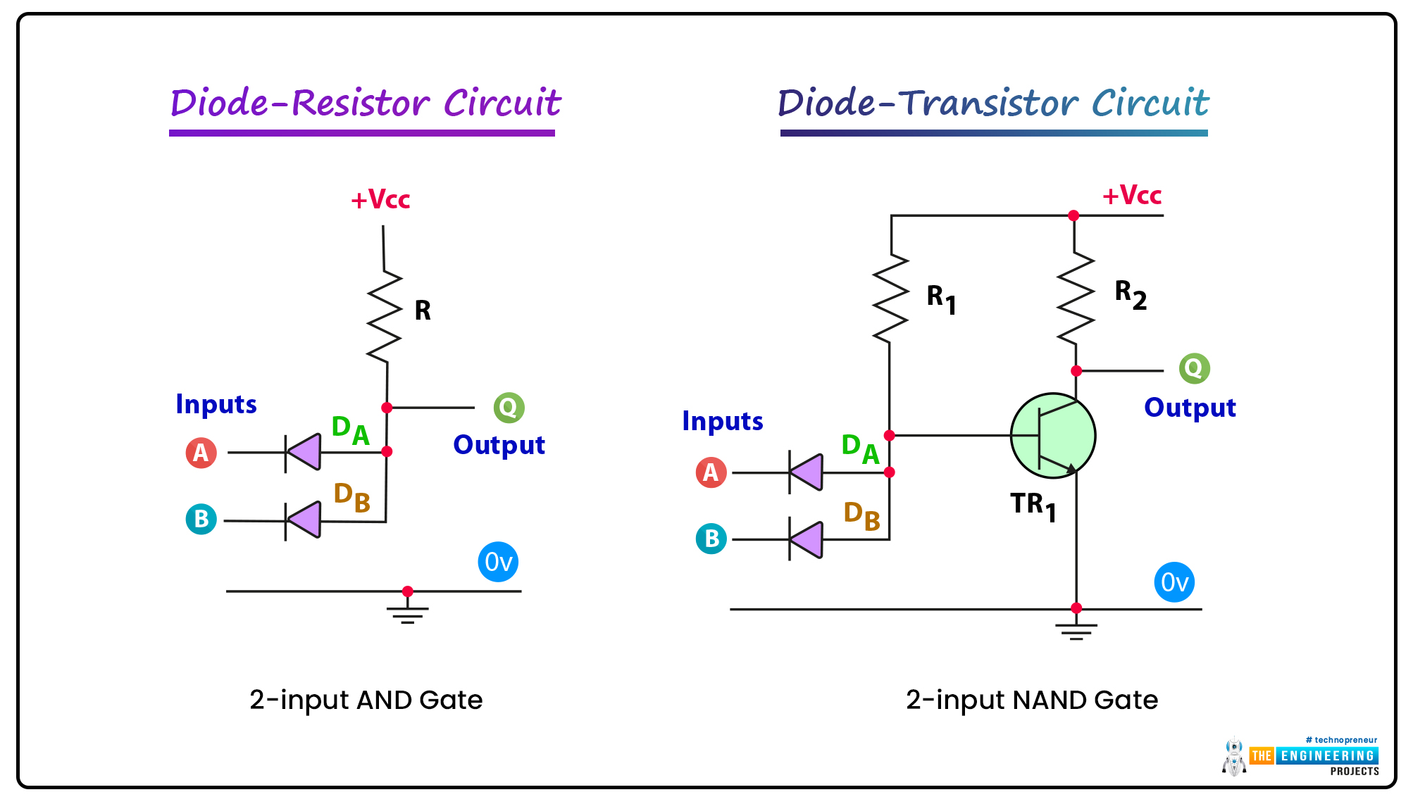
As you can see in the above figure, these circuits are quite easy to design, as simply using diodes, resistors, and transistors. But these circuits are not used in commercial ICs because of their high power loss(pull-up resistor) and gate delay(propagation delay). That's why, CMOS and TTL are considered the better option to design digital logic gates.
TTL Logic Gates
In TTL Logic Gates, NPN and PNP transistors are used for designing logic gates. The ideal TTL logic gate is the one that gives the LOW(0) Logic at 0V and HIGH(1) Logic at 5V. In a real TTL Logic Gate, the logic will be considered LOW(0), if the voltage level lies between 0-0.8V and the logic will be considered HIGH(1), if the voltage level is in the range of 2-5V. The voltage level between 0.8-2V is considered a "no man's land" and normally external pull-up or pull-down resistors are used to avoid this region. Examples of TTL Logic Gates ICs are 74Lxx, 74LSxx, 74ALSxx, 74HCxx, 74HCTxx, 74ACTxx etc. The switching voltage varies from group to group according to their internal structure and material used.
CMOS Logic Gates
In CMOS Logic Gates, FET(Field Effect Transistor) and MOSFET are used to design the logic gates. CMOS logic gates provide a LOW(0) logic, if its voltage is in the range of 0-1.5V and it will give HIGH(1) logic, if it's in the range of 3-18V. The below table shows the voltage levels of both TTL and CMOS logic Gates:
| Logic Gates |
LOW(0) |
HIGH(1) |
| TTL |
0-0.8V |
2-5V |
| CMOS |
0-1.5V |
3-18V |
Now, let's have a look at the Types of Logic Gates:
Types of Logic Gates
- There are numerous types of Logic gates available based on the quantity of input/output channels and the type of logic to be applied.
- Based on the specified logic, gates are divided into 3 basic types, i.e.
- AND Gate.
- OR Gate.
- NOT Gate.
- These 3 basic gates are the building blocks of all advanced logic gates. So, we can design any advance logic gate with these 3 basic logic gates.
- The most commonly used Advance Logic Gates are:
- NAND Gate.
- NOR Gate.
- XOR Gate.
- XNOR Gate.
- The above-mentioned 7 logic gates are the most commonly used ones. Following logic gates are not that common but are in practice:
- MIN(Minimum) Logic Gate.
- MAX(Maximum) Logic Gate.
- INH(Inhibit) Logic Gate.
- MAJ(Majority) Logic Gate.
- IMP(IMPLY) Logic Gate.
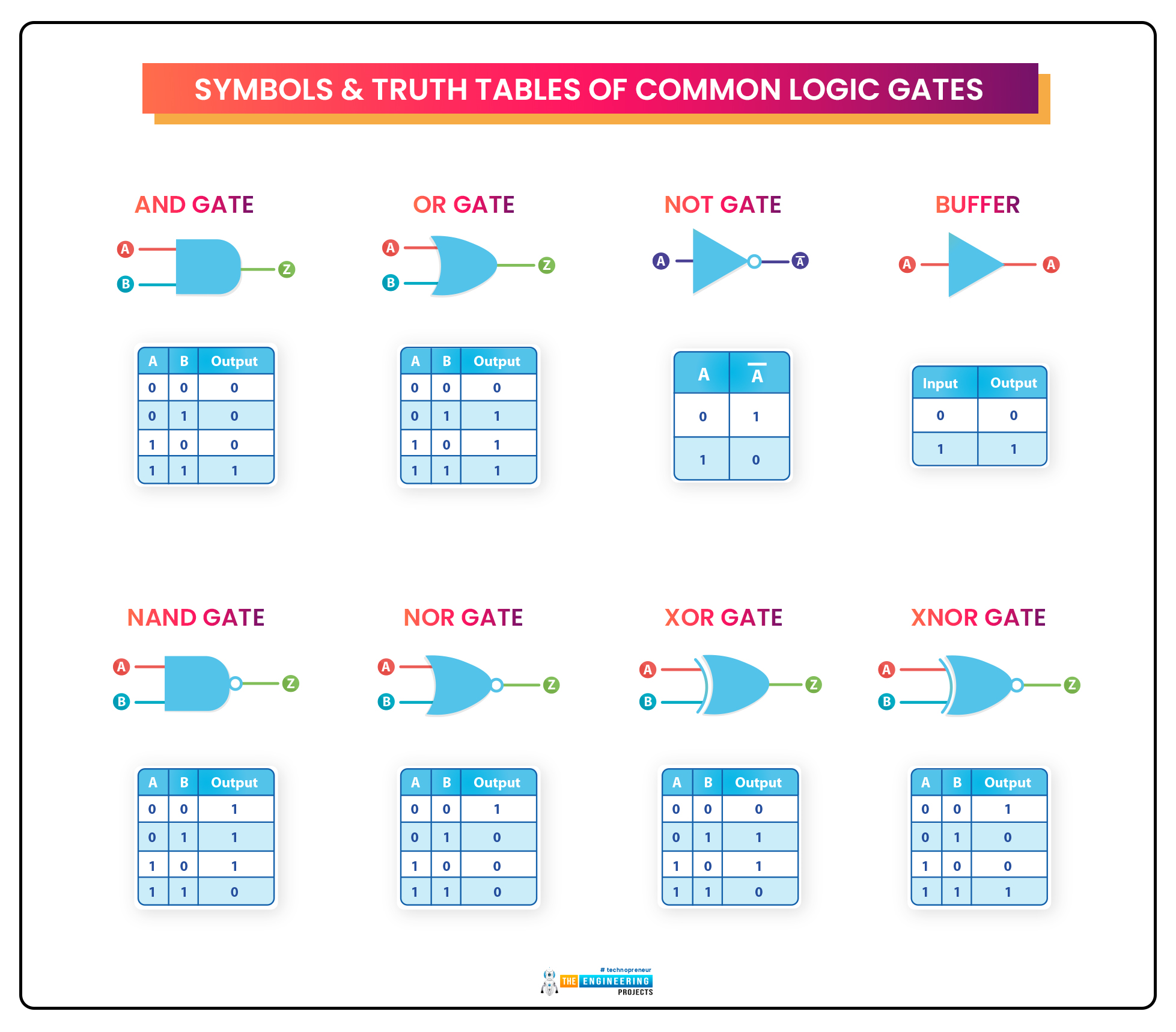
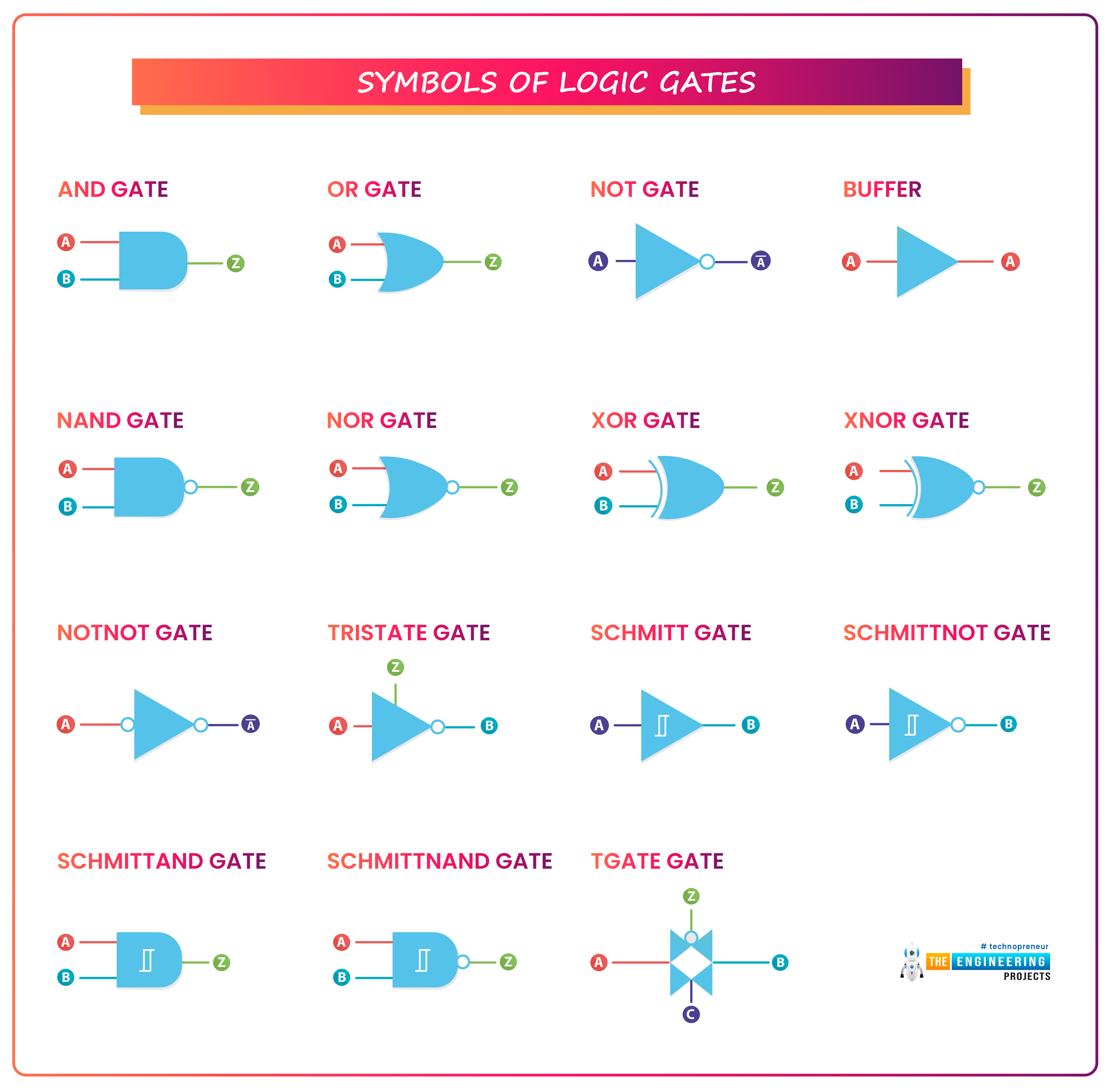
It's quite difficult to cover all these gates in a single lecture. So, we will only discuss the basic 7 gates i.e. AND, OR, NOT, NAND, NOR, XOR and XNOR. Today, we will have a brief overview of these 7 logic gates but in the upcoming lectures, we will cover each one of these individually in full detail. Here are the symbols of few logic gates:
So, let's get started:
AND Logic Gate
- AND Gate is a basic logic gate and gives HIGH output, when all of its Inputs are HIGH and generates LOW output, if any of its Inputs got LOW.
- The AND Gate performs the Logical conjunction. We denote it with the DOT between the inputs i.e. A.B = Y where A & B are the inputs and Z is the output.
- The Inputs in AND Gate is always more than one i.e. Inputs >= 2 and it will always generate a single output.
- The logical symbol of the AND gate is shown in the below figure:
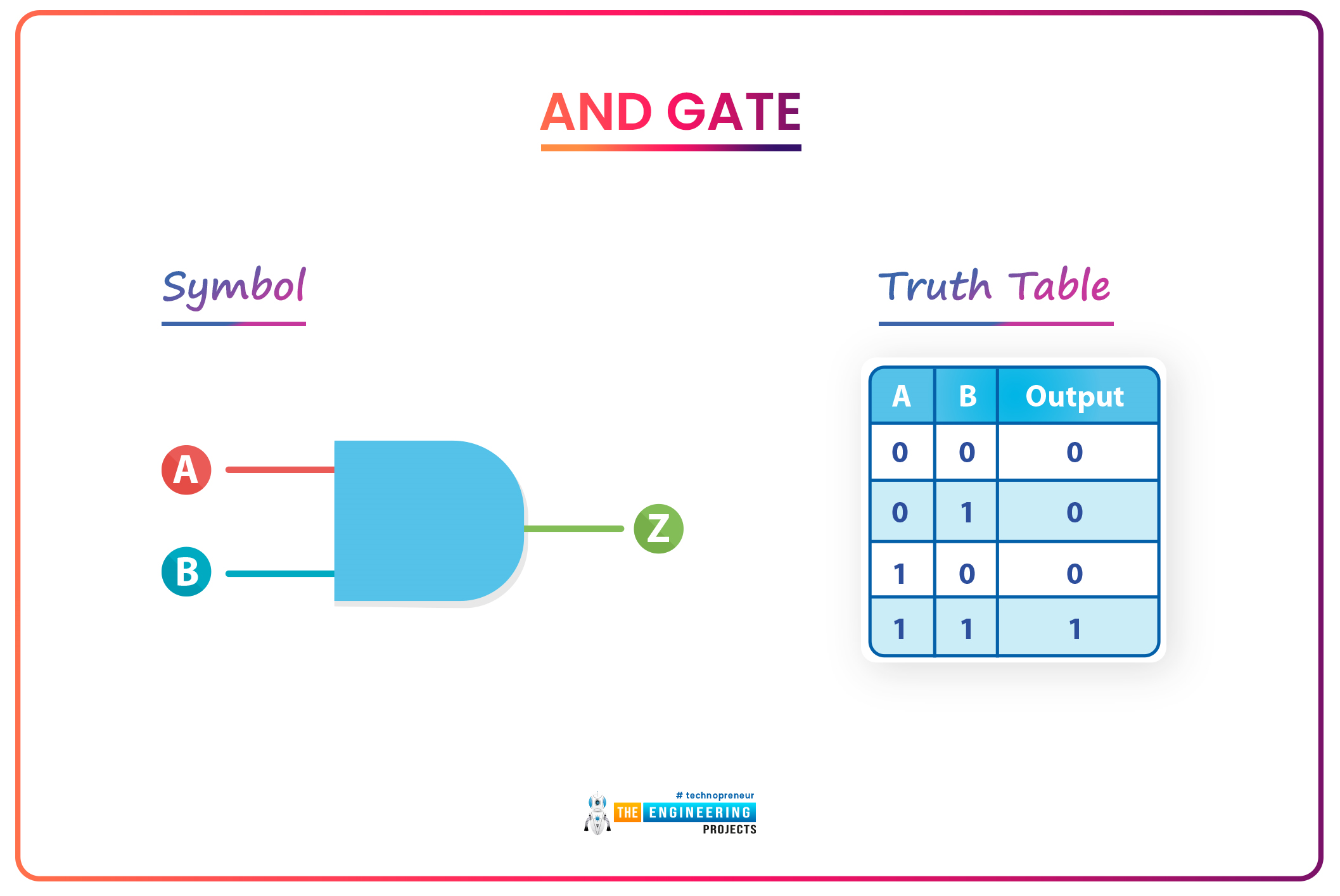
Truth Table:
- Here's the truth table of AND gate in tabular form:
| A | B | A.B |
| 0 | 0 | 0 |
| 0 | 1 | 0 |
| 1 | 0 | 0 |
| 1 | 1 | 1 |
As you can see in the truth table of AND Gate, the Output is 1 only when both of its inputs are 1, otherwise, it's 0.
Proteus Simulation of AND Gate
Proteus has an AND Gate component in its components library. We are going to use it to verify the truth table of AND Gate. We will use the following components for designing this AND Gate Simulation:
- AND Gate
- LED
- Logic Toggle
- Ground Terminal
Here's the Proteus simulation of all possible states of the AND Gate with 2-inputs:
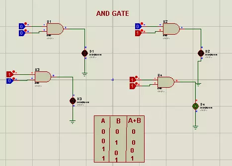
- I have placed a Logic State at the inputs of the AND gate and an LED at the output.
- The LED glows only when both of its Inputs are 1(HIGH).
OR Gate
- OR gate performs the Disjunction Logic on the inputs i.e. The output will be 1(HIGH), if any of its Inputs is 1(HIGH) and the output will be 0(LOW), if all of its Inputs are 0(LOW).
- OR Gate is denoted by a plus sign "+" between the inputs i.e. A+B = Y, where A & B are the inputs and Y is the output.
- Identical to AND Gate, OR Gate also has a minimum of two inputs and only one output.
- The OR Gate Symbol is shown in the below figure:
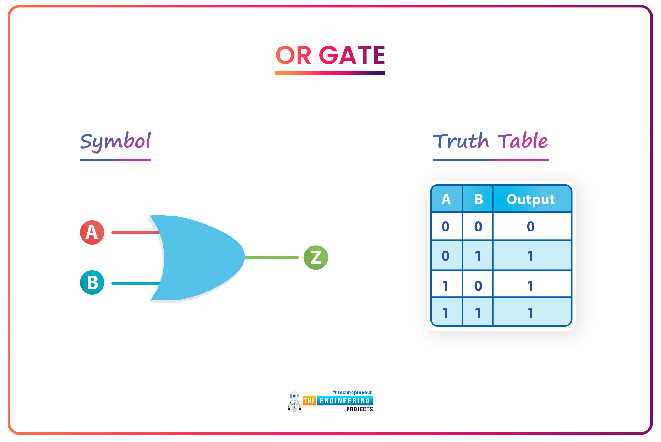
Truth Table:
- Here's the truth table for the OR Gate:
| A | B | A+B |
| 0 | 0 | 0 |
| 0 | 1 | 1 |
| 1 | 0 | 1 |
| 1 | 1 | 1 |
In the case of OR Gate, the output is LOW, only when all of its inputs are LOW, otherwise its HIGH.
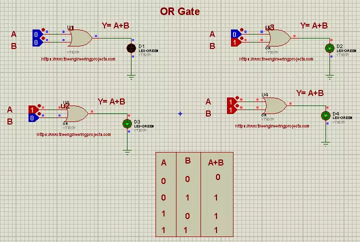
Proteus Simulation of OR Gate
- The simulation is quite the same as that of the AND gate, we simply replace the AND Gate with OR Gate, present in the Proteus components library.
- The below figure shows that the output LED is OFF, only when both inputs of OR gate are LOW.
NOT Gate
- In Logic Circuits, the NOT Gate performs the inversion.
- This is a unary logic Gate that implies it has only one input and a single output.
- The output of NOT Gate is denoted by a Bar or Complement on the input symbol i.e. If the input is A, the output will be A'.
- Here's the symbolic representation of NOT Gate:
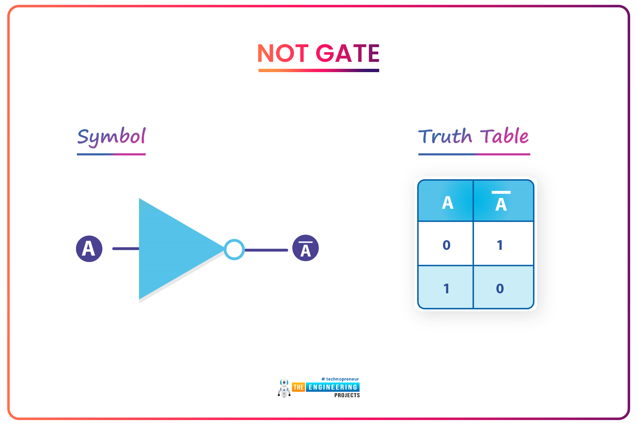
Truth Table:
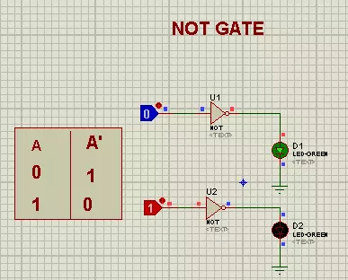
- Here's the truth table of NOT gate, quite simple isn't it?
| A | B |
| 0 | 1 |
| 1 | 0 |
Proteus Simulation of NOT Gate
- Grab the NOT Gate from the Proteus components library.
- Attach LED and logic toggle at output and input respectively.
- Here are the results:
So, today we discussed the basic logic gates i.e. AND, OR and NOT Gate and simulated them in Proteus. In upcoming lectures, we'll use these gates to design advance gates and circuits. Take care!!!