


Designing Custom Aluminum Electronics Enclosures: DFM, Thermal, and EMI Guide


Enclosures in modern high-performance embedded systems, industrial IoT devices, and RF hardware are not mere decorative dust covers. The components are becoming increasingly dense with a lot of high-power processing, GaN/SiC power stages, and high-frequency transceivers in a very small area. This type of physical compactness gives rise to severe thermal issues and risk of electromagnetic interference (EMI) that may lower the quality of signals or make the device perform in a throttled way. A bespoke enclosure made out of aluminum can be a multi-functional part of the system providing protection for electronics while allowing dissipation of heat by convection and also acting as an EMI-enclosing Faraday cage in a typical electronics packaging environment.
Metal stamped sheet and die casting offer an attractive way to manufacture gadgets for the masses whereas solid-billet CNC-machined aluminum is the go-to route for making tough industrial hardware, aerospace components, and high-precision functional prototypes. CNC machining offers equal mechanical strength in all directions, excellent heat dissipation, and geometric accuracy of just a micrometer level without needing tooling molds which are cost intensive and have long lead times.
Making a functional and affordable enclosure basically needs an understanding and good implementation of three engineering aspects: direct thermal management, efficient EMI attenuation, and a clever Design for Manufacturability (DFM).
Material Selection: 6061-T6 vs. 5052 vs. 7075
The selection of the appropriate aluminum grade is the starting point that sets the stage for the performance in thermal dissipation, structural rigidity, tool and component wear, and also machining rates. Majority of the time, one can find custom electronics enclosures made from only three types of alloys:
| Table 1 | |||||
|---|---|---|---|---|---|
| Alloy & Temper | Thermal Conductivity (k) | Yield Strength | Machinability Rating | Anodizing Response | Primary Application |
| 6061-T6 | ~167 W/(m·K) | 276 MPa | Excellent | Excellent (Clear & Color) | General CNC chassis, integrated heat spreaders |
| 5052-H32 | ~138 W/(m·K) | 193 MPa | Fair (gummy chip formation) | Fair (often yellowish tint) | Sheet-metal hybrid panels, stamped covers |
| 7075-T6 | ~130 W/(m·K) | 503 MPa | Superior | Good (darker, harder base) | High-shock aerospace housings, structural brackets |
| Thanks !!! | |||||
6061-T6: The Go-To Industry Workhorse
One reason 6061-T6 is a popular choice among machinists for housing electronics is that it gives the best balance for almost 90% of products. Its high thermal conductivity of about 167 W/(m·K) makes it a perfect heat dissipation medium, the hot silicon chips' heat is quickly moved, and it is also evenly distributed across the external metal parts of the enclosure. It can be cut cleanly with common carbide end-cutters, debris is well controlled in a consistent manner after machining, and stress is hardly induced when machining using stress-relieved blanks.
When to Upgrade to 7075-T6 or Switch to 5052
If an enclosure acts as a stressed structural member in aerospace hardware exposed to high-G loads and severe vibration, 7075-T6 supplies nearly double the yield strength of 6061-T6. The trade-offs are higher material stock costs and a 22% drop in thermal performance. On the other hand, 5052 is best reserved for hybrid designs where a thick CNC-machined base tub pairs with a simple, bent-sheet access cover.
Thermal Architecture: Integrating Heat Sinks Directly into the Chassis
Mounting off-the-shelf extruded heat sinks onto an enclosure using thermal interface materials (TIM) introduces stacked thermal boundary resistances and inflates your assembly bill of materials. A far cleaner engineering approach is direct-to-chassis cooling, where cooling fins and internal thermal pedestals are milled directly into the aluminum chassis itself.
Machining Exterior Convective Fins: Practical Rules
When milling fin arrays into solid billet with rotary endmills, cutting physics dictates explicit height-to-gap ratios:
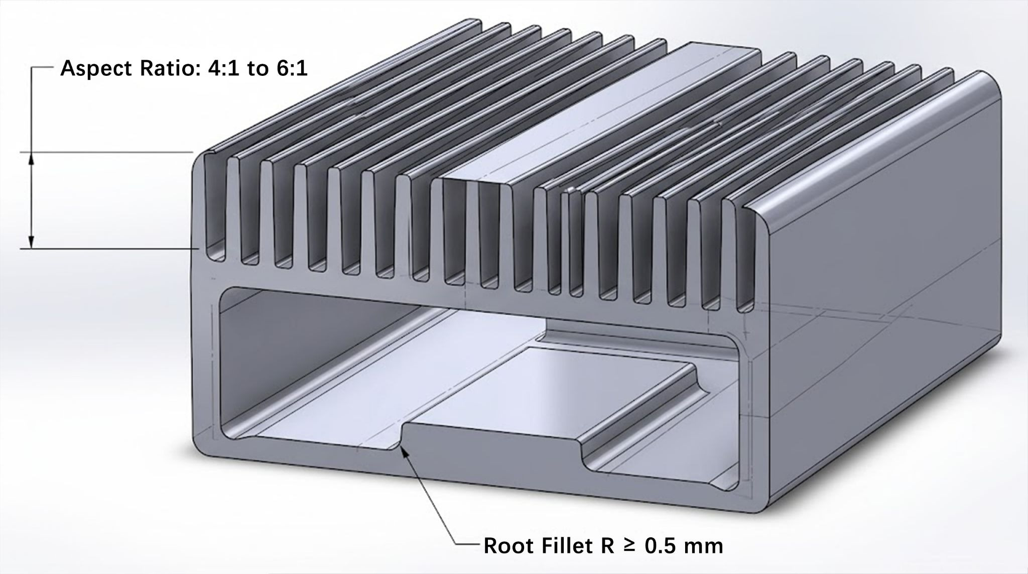
1. Aspect Ratio Limitations: fin height and gap dimension ratio must be 4:1 to 6:1. Exceeding 8:1 ratio would necessitate a long reach tool that can achieve high length-to-diameter ratios. These types of thin cutters tend to deflect when subjected to cutting forces thereby, making the cutting surface inconsistent and tools prone to damage as well as chatter.
2. Fin Thickness & Draft Angle: fin thickness should be kept minimum of 1.5 mm and it is better that it is more than or equal to 2.0 mm. Thin fins get deformed due to side-milling loads and result in irregular wavy patterns. Adding a subtle 1° to 2° draft angle speeds up chip clearing on deeper passes.
3. Root Fillet Radii: Never design sharp 90° transitions where fins meet the main housing base. Specify a root radius of R ≥ 0.5 mm to 1.0 mm. These small changes can help release stress points and allow machinists to use standard radius-tipped bull-nose endmills at even faster speeds.
Thermal Interface Pedestals
To channel heat away from high-power ICs into the outer casing, machine dedicated pedestals that rise directly from the floor of the inner pocket. For proper thermal contact, specify a surface roughness of Ra ≤ 0.8 μm and a flatness tolerance within 0.05 mm across the pedestal face. This keeps microscopic air gaps to a minimum without driving up machine cycle time with slow, secondary lapping operations.
[Figure 1 description: CNC aluminum enclosure with integrated heat sink fins (4:1 to 6:1 aspect ratio) and thermal pedestals.]
EMI/EMC Shielding: Enclosure Geometry and Sealing Mechanics
To ensure electromagnetic compatibility, the enclosure needs to perform as a good conductor of electromagnetic waves and should be able to block their access. At sub-gigahertz frequencies, walls of solid aluminum can give attenuation figures that are in excess of 100 dB. In actual hardware, shielding failures hardly ever originate in metal thickness, they mostly occur at seams, splits, or places where covers meet surfaces.
Seam Radiation and Slot Antennas
Microscopic gaps along a bolted seam function as resonant slot antennas. If the maximum length of an opening approaches a half-wavelength (λ/2) of your operating frequency, RF energy radiates outward unobstructed. For instance, at 5 GHz, a gap of just 30 mm radiates efficiently. To maintain attenuation figures > 60 dB in high-frequency hardware, gap dimensions along joints must stay below λ/20.
Tongue-and-Groove Joint Geometry
Simple one-face flanges are inadequate if one needs to achieve a good degree of attenuation of RF signals or meet outdoor IP ratings:
l The Tortuous Path: Machine an interlocking tongue-and-groove (labyrinth) profile along the perimeter joint. This causes electromagnetic radiation to reflect multiple times inside the mechanical channel, significantly limiting RF leakage compared to a flat butt joint.
l Gasket Channel Tolerances: When using conductive elastomer gaskets (such as silicone filled with silver-plated aluminum particles), precision-mill the gasket groove to match the gasket volume. Maintain groove depth and width tolerances within ±0.05 mm. This ensures a nominal gasket compression of 20% to 30% under bolt tension without pinching or over-compressing the material.
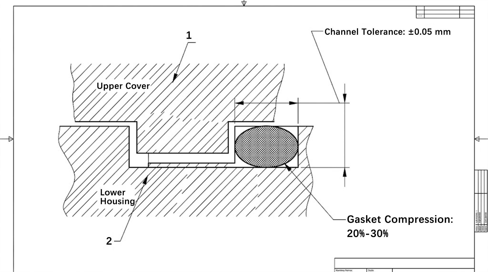
[Figure 2 description: Cross-section of a tongue-and-groove RF joint detailing gasket compression (20% to 30%).]
Fastener Spacing Along Flanges
Loose or widely spaced bolts allow thin lids to bow outward between fasteners, creating invisible RF escape slits. A reliable mechanical rule of thumb is:
Pitch ≤ min(20 × Flange Thickness, λ/20)
Placing fasteners at intervals between 25 mm and 40 mm ensures uniform, continuous contact pressure along the conductive perimeter gasket.
Core DFM Practices for Precision CNC Machining
Translating a 3D CAD model into clean metal parts requires designing geometries that minimize cycle time, avoid tool breakage, and run in as few setups as possible. When dealing with tight dimensional tolerances and short prototyping windows, partnering with an experienced rapid prototype and low-volume production manufacturer like LS Manufacturing ensures that tight machining tolerances, geometric checks, and quick-turn deliveries align smoothly with design goals.
1. Optimize Internal Pocket Corners
Rotary milling cutters cannot cut sharp, square 90° internal vertical corners:
l The Rule: Always make the internal corner radius larger than the radius of the cutting tool. If roughing out pockets with a 6 mm diameter endmill (3 mm radius), specify an internal corner radius of R ≥ 3.5 mm to 4.0 mm.
l Why It Matters: If the corner radius matches the tool radius exactly, the cutter contacts material across a full 90° arc at once, spiking cutting force, causing chatter, and breaking tool tips. An oversized radius lets the CNC machine sweep around the turn at a steady feed rate.
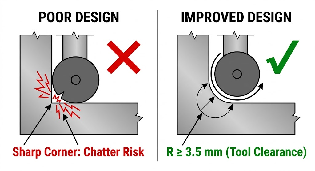
[Figure 3 description: DFM comparison of CNC toolpath engagement: sharp 90° corners versus radiused transitions.]
2. Manage Cavity Depth vs. Tool Deflection
Deep internal pockets inflate machining costs rapidly:
l Restrict internal cavity depth to ≤ 4× tool diameter.
l The more that pocket cutting goes beyond four times tool diameter, the more the machine operator has to drop the spindle speed and feed rate to keep tool deflection from happening. Such deflection will cause the pocket walls to become conical (e.g., narrower near the floors and wider at the top), besides causing poor surface quality.
3. Maintain Structural Wall Thickness
To keep walls from vibrating or warping under heavy cutting passes:
l For standard internal pockets, keep the wall thickness at least 1.5 mm and for outer walls over 50 mm high, use 2.0 mm thick walls.
l Designing walls thinner than 1.0 mm requires delicate, low-depth finishing passes, which increases machine run time and part cost.
4. PCB Mounting Boss Alignment
Ensure all PCB mounting bosses maintain a true position tolerance within ±0.025 mm relative to primary datums. Too much positional error causes mounting screws to push against the circuit board holes, transferring shearing force onto the fiberglass PCB. As a result, surface mount solder joints might be cracked when the component goes through thermal cycling.
Surface Finishing and the Grounding Paradox
Anodizing is the standard finish for aluminum housings not only because it gives the product a nice look, it also protects the metal from corrosion and prevents scratches. Still, the process involves chemical reaction of raw aluminum to produce a new material-anodized aluminum oxide (Al2O3) film-which incidentally is an electrical insulator.
A fully anodized housing interrupts electrical continuity across split lines and ruins EMI shielding. Resolving this issue requires a targeted masking and dual-finish strategy:
1. Selective Masking: To cover up conductive gasket grooves you could use masking dots, silicone plugs, or custom fixtures. You can also cover up PCB mounting standoffs and threaded grounding bosses in this way.
2. Exterior Protective Anodizing: To achieve both wear and environmental protection all the exposed outer surfaces should be covered with MIL-A-8625 Type II (decorative) or Type III (hardcoat) anodizing.
3. Conductive Chemical Conversion: Coat the unanodized, masked internal areas with a chemical conversion coating (MIL-DTL-5541 or SurTec 650). This thin passivation layer prevents corrosion while preserving a low surface contact resistance (< 2.5 mΩ), ensuring solid chassis grounding.
4. Account for Coating Thickness: Make sure that when parts are made, any changes in size caused by coatings or processes are already taken into account in your drawings and specifications. Type II anodizing typically adds an outward growth of 10 μm to 15 μm, while Type III hardcoat can add 25 μm to 50 μm per side. Make sure critical H7 alignment holes and precision threaded holes are masked or tapped slightly oversize to avoid binding during final assembly.
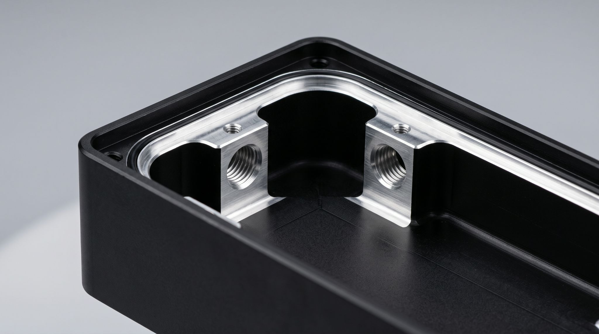
[Figure 4 description: Dual-surface finish: external protective anodizing with selective MIL-DTL-5541 conductive coating for grounding.]
If one manages these multidisciplinary design parameters very early on in the CAD modeling phase this will help the design to have all the properties of the electrical performances, thermal dissipation and even the raw machinability. If these are the only things that one thinks of when designing an RF enclosure, the result will only be good on paper, which is not the case in the real world where things are more complex. That means, for a high quality RF enclosure, some other things that must be considered are the cutting tool paths, wall deflections, RF seam physics and conductive plating margins; these are the things that will give the concept life and turn it into a robust, high-yield enclosure that will be ready for deployment in the real world.

Comments
0