FDV301N N-channel MOSFET Datasheet, Pinout, Features & Applications

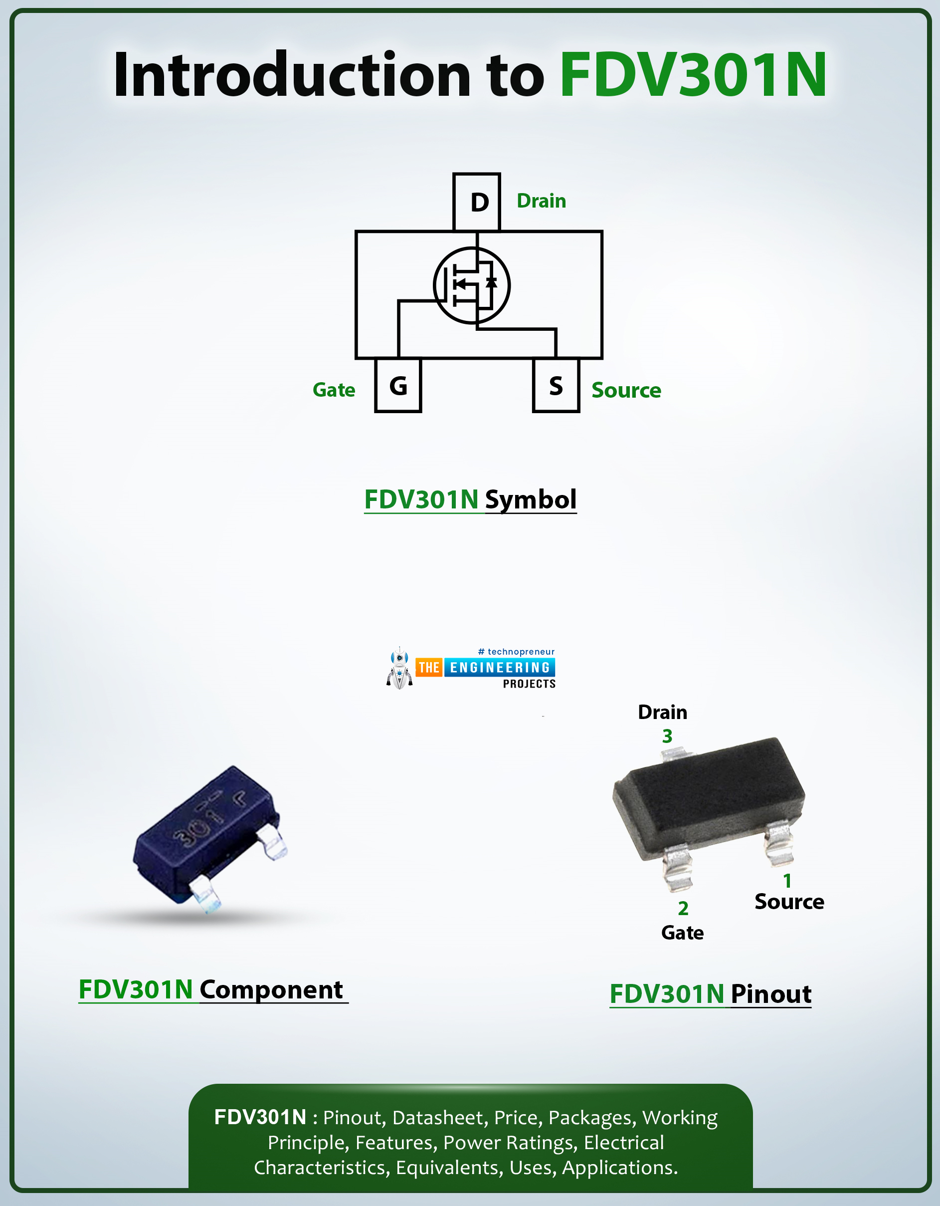
Hello Everyone! I welcome you on board. Happy to see you around. In this post today, I’ll walk you through the Introduction to FDB301N.

The FDV301N is an N-channel MOSFET using Fairchild's proprietary and high cell density, DMOS technology. The cell’s high density helps to minimize the on-state resistance. This device is mainly developed for low-voltage applications. This N-channel MOSFET replaces different digital transistors and provides different bias resistor values.

I suggest you read this post all the way through as I’ll detail the complete Introduction to FDV301N covering datasheet, pinout, features and applications. Let’s jump right in.

Introduction to FDV301N

  • The FDV301N is an N-channel MOSFET mainly used for switching and low-voltage applications.
  • It carries low on-state resistance and can be used in place of different transistors for a range of applications.

  • This device contains three terminals named gate, drain, and source. The source is the terminal from which electrons enter the channel and drain is the area where electrons leave the channel. While gate terminal is used for biasing the device.
  • The MOSFETs are mainly divided into two main types i.e. N-channel MOSFET and P-channel MOSFET. The N-channel MOSFETs carry electrons as major charge carriers and P-channel MOSFETs contain holes as the major charge carriers.
  • The movement of electrons is better than the movement of holes, making N-channel MOSFETs better than P-channel MOSFETs for a range of applications, especially for high-load applications.
  • The drain-source voltage of this device is 25V and gate-source voltage is 8V and maximum power dissipation is 0.35W. This is the amount of power it dissipates during the working of this device.

FDV301N Datasheet

It’s wise to go through the datasheet before you apply this component to your electrical project as using this datasheet you can get a hold of the main characteristics of the device. Click the link below to download the datasheet of FDV301N.

FDV301N Pinout

The following figure shows the pinout diagram of FDV301N. This chip comes with three terminals called source, gate, and drain.
Pin Description of FDV301N
Pin No. Pin Description Pin Name
1 Electrons enter the channel through the source terminal Source (S)
2 Used for biasing the device Gate (G)
3 Electrons leave the channel through the source terminal Drain (D)

FDV301N Features

The following are the main features of FDV301N.
  • The RDS (on-state resistance) is a resistance between drain and source terminal that is 5? at gate-source voltage VGS of 2.7V and it’s 4? at VGS of 4.5V.
  • The gate-source voltage (VGS-th) is 8V
  • Drain Source Voltage (VDS) is 25V
  • Continuous Drain Current (ID) is 220mA
  • Level gate drive requirements are very low, helping direct operation in 3V circuits.
  • The high-density cell process ensures low on-state resistance RDS (ON).
  • This device is reliable and rugged.
  • The operating and storage temperature range is -55C to 150C.
  • Comes in a compact industry-standard SOT-23 surface-mount package.

FDV301N Applications

This N-channel MOSFET chip is used in the following applications.
  • Incorporated in low voltage low current applications.
  • Employed as switching devices in electronic control units.
  • Used in automotive electronics.
  • Used as power converters in modern electric vehicles.
  • Used in servo motor control.

That’s all for today. Hope you’ve got a brief insight into the Introduction to FDV301N. If you have any query, you can share your comment in the section below, I’ll help you the best way I can. Feel free to share your valuable feedback and suggestions around the content we share so we keep producing quality content customized to your exact needs and requirements. Thank you for reading the article.

IRF520 MOSFET Datasheet, Pinout, Features & Applications

Hi Guys! Hope you’re well today. Happy to see you around. Today, I’ll walk you through the Introduction to IRF520.

The IRF520 is an N-channel power MOSFET mainly used for switching and amplification purposes. It comes with a breakdown voltage of around 100V and a low gate threshold voltage is 4V, making it an ideal pick for microcontroller applications.

I suggest you read this post all the way through as I’ll detail the complete Introduction to IRF520 covering datasheet, pinout, features, and applications. Let’s get started.

Introduction to IRF520 MOSFET

  • The IRF520 is an N-channel power MOSFET mainly used for switching and amplification purposes.
  • It comes with three terminals named: gate, source, and drain and is available in the TO-220 package.
  • It is important to note that the gate terminal is electrically insulated and contains no current and is normally called an Insulated Gate FET (IG-FET).

  • As it’s an N-channel MOSFET so here major charge carriers are electrons as opposed to P-channel MOSFET where major carriers are holes.
  • The movement of electrons is better than the movement of holes, making N-channel MOSFET better than P-channel MOSFET.
  • Due to better movement of electrons, N-channel MOSFETs with high loads remain cool while P-channel MOSFETs turn hot in the presence of high loads.
  • The major charge carriers i.e. electrons enter the channel through the source terminal while they exit the channel through the drain terminal. And the gate terminal controls the biasing of this MOSFET.
  • This N-channel MOSFET comes with low on-state resistance of around 0.27 ohm, allowing it to dissipate less energy as heat and consequently increasing the efficiency of the device.
  • IRF520 contains a low threshold voltage of around 4V which projects it can be turned on with 5V on the GPIO pins on the microcontroller.
  • This chip comes with a decent switching speed, making it an ideal pick for DC-DC converter circuits.
  • The continuous drain current (ID) of this device is 9.2A while the drain-to-source breakdown voltage is 100V. The Rise time is 30ns and the fall time is 20nS.

IRF520 Datasheet

Before you apply this component to your electrical project, it’s wise to scan through the datasheet of the component that features the main characteristics of the device. Click the link below to download the datasheet of IRF520.

IRF520 Pinout

The following figure shows the pinout diagram of IRF520 Mosfet. The IRF520 comes in three terminals named Gate, Drain, and Source.
Pin Description of IRF520
Pin No. Pin Description Pin Name
1 Used for biasing the device Gate
2 Electrons leave the channel through a drain terminal Drain
3 Electrons enter the channel through the source terminal Source

IRF520 Features

The following are the main features of IRF520 mosfet.
  • N-Channel Power MOSFET
  • Continuous Drain Current (ID) = 9.2A
  • Drain to Source Breakdown Voltage = 100V
  • Rise time is 30ns and the fall time is 20nS.
  • Drain Source Resistance (RDS) = 0.27 Ohms (also known as on-state resistance)
  • Since it contains low threshold voltage, it is commonly employed with Arduino applications.
  • Gate threshold voltage (VGS-th) = 4V (max)
  • Available Package = TO-220 package

IRF520 Applications

The following are the main applications of this device.
  • Employed to control the speed of motors
  • Used in converters or Inverter circuits
  • Used in high power devices
  • Incorporated in high-speed switching applications
  • Used in LED dimmers or flashers

That’s all for today. Hope you’ve got a brief insight into Introduction to IRF520 mosfet. If you’re unsure or have any questions, you can approach me in the section below. I’d love to help you the best way I can. Feel free to share your valuable feedback and suggestions around the content we share so we keep coming back with quality content customized to your exact needs and requirements. Thank you for reading the article.

BSS138 MOSFET Datasheet, Pinout, Features & Applications

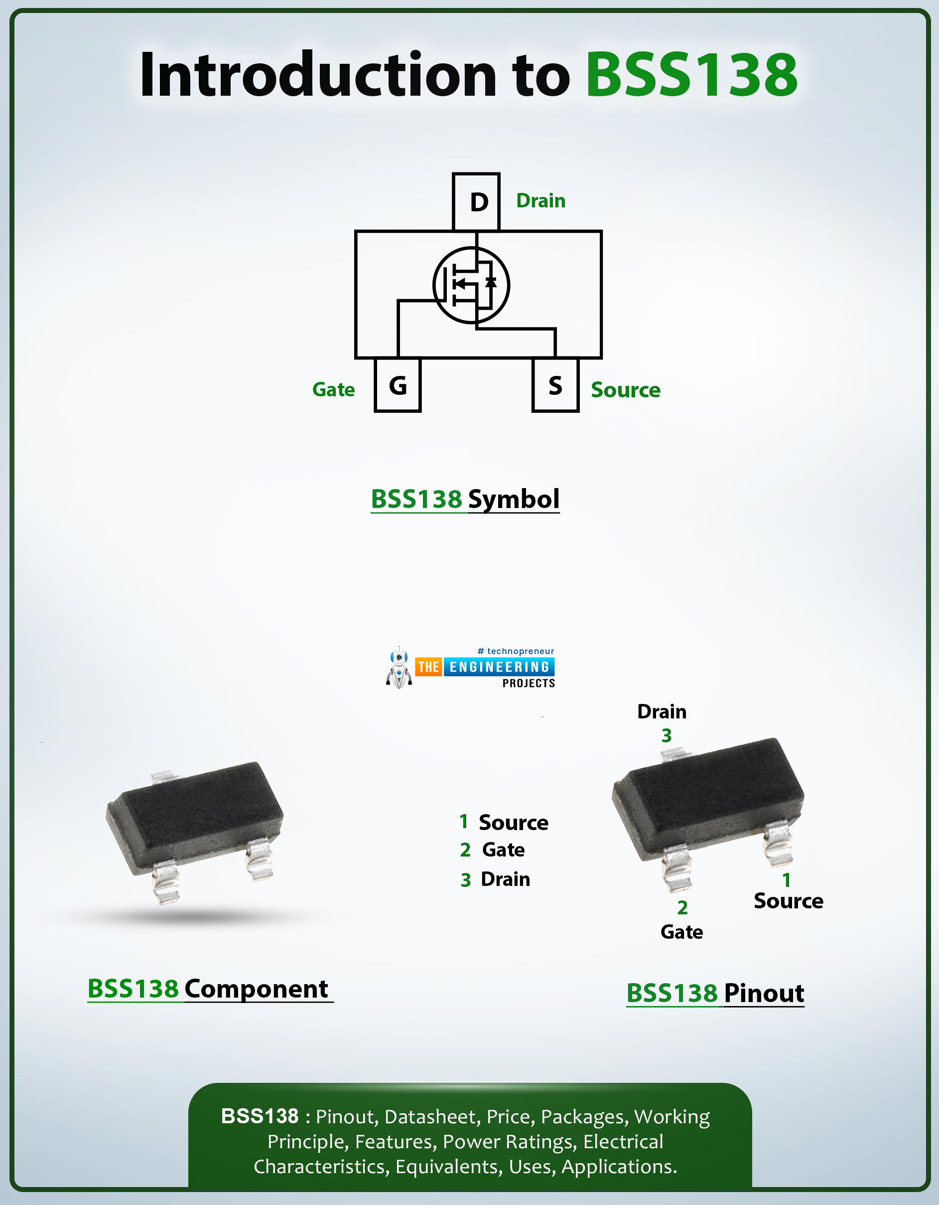
Hi Everyone! Hope you’re well today. I welcome you on board. In this post today, I’ll detail the Introduction to BSS138.

The BSS138 is an N-Channel Logic Level Enhancement Mode Field Effect Transistor that is available in surface mount package SOT-23. It features a low input capacitance of around 40pF and a low on-state resistance of around 3.5. High switching speed and low threshold voltage make this device an ideal pick for level shifter circuit applications.

I suggest you read this post all the way through as I’ll walk you through the complete Introduction to BSS138 covering datasheet, pinout, features, and applications. Let’s jump right in.

Introduction to BSS138

  • The BSS138 is an N-Channel MOSFET mainly used in low current and low voltage switching applications.
  • It contains three terminals called, drain, source, and gate. At times the body is also included in the terminals, making it a four-terminal device.

  • It is important to note that the gate terminal is electrically insulated and contains no current and is normally called an Insulated Gate FET (IG-FET).
  • MOSFETs are categorized into two main types i.e. N-channel MOSFET and P-channel MOSFET. This chip BS138 falls under the category of N-channel MOSFET where electrons are major carriers. While holes are major carriers in P-channel MOSFETs.
  • The electron movement is better than the hole movement. The reason, N-channel MOSFETs are preferred over P-channel MOSFETs for a range of applications.
  • During working with high loads the P-channel MOSFETs turn hot while the N-channel MOSFETs remain cool.
  • BSS138 comes in a continuous drain current of around 200mA and drain-source VDS voltage is 50V.
  • The on-state resistance of this chip is 3.5, while the turn-off and turn-ON time is 20ns each.
  • The compact and robust nature of this device makes it an ideal choice for portable applications including power management circuits and cell phones.
  • The BSS138 is costly compared to its alternative 2n7002. Picking the alternative, you have to compromise with the threshold voltage and on-state resistance.

BSS138 Datasheet

Before you incorporate this component into your electrical project, it’s better to scan through the datasheet of the component that highlights the main characteristics of the device. You can download the datasheet of BS138 by clicking the link below.

BSS138 Pinout

The following figure shows the pinout diagram of BSS138. This device contains three terminals called source, drain, and gate.
Pin Description of BSS138
Pin No. Pin Description Pin Name
1 Electrons enter the channel through the source terminal Source (S)
2 Controls the biasing of the component Gate (G)
3 Electrons leave the channel through the drain terminal Drain (D)

BSS138 Features

The following are the main features of BSS138.
  • Logic Level N-Channel MOSFET
  • Turn ON and Turn OFF time = 20ns each
  • Continuous Drain Current (ID) = 200mA
  • Comes in low on-state resistance
  • Gate threshold voltage (VGS-th) = 0.5V
  • On-state Resistance = 3.5?
  • Drain Source Voltage (VDS) = 50V
  • Gate threshold voltage (VGS-th) = 1.5V
  • Available Package = SOT23 SMD

BSS138 Alternatives

The following are the alternatives to BSS138.
  • IRF540N
  • IRF3205
  • IRF1010E
  • 2N7000
  • BS170N
Before you incorporate these alternatives, double-check the pinout of these equivalents as the pinout of the alternatives might differ from the pinout of BSS138.

BSS138 Applications

This chip is used in the following applications. Used in automotive electronics.
  • Employed as switching devices in electronic control units.
  • Incorporated in low voltage low current applications.
  • Used in automotive electronics.
  • Used as power converters in modern electric vehicles.
  • Used in servo motor control.

That’s all for today. Hope you’ve got a brief insight into the Introduction to BSS138. If you have any questions, you can approach me in the section below, I’d love to help you the best way I can. You’re most welcome to share your valuable feedback and suggestions around the content we share so we keep sharing quality content customized to your exact needs and requirements. Thank you for reading the post.

T Flip Flop Circuit Diagram in Proteus ISIS

Hey Learners! I welcome you on the behalf of The Engineering Projects. I hope you are doing Great. If you are seeking for the best information about the T Flip Flop along with some small concepts and the Practical Performance, then you are at the right article. In this session you will get the following topics:
  • What are T Flip Flops?
  • What are the Functions of Preset and Clear Input in T Flip Flop?
  • How can we Design the Truth Table of T Flip Flop?
  • How can you perform the T Flip Flop simulation in very simple and useful way?
Moreover, you will also get some pieces of information in DID YOU KNOW sections. so without wasting time, lets Jump into the answer of 1st Question.

T Flip Flop

T Flip Flop belongs to the family of Flip Flops and Latches and we define the T Flip Flop as:
"T Flip Flops are bi-stable sequential Logic Circuits that are the modification of SR Flip Flops and contain just one input called T and two outputs called Q and Q' and a Clock input in the circuit. "
The Circuit is similar to the JK Flip Flop but the inputs are connected with the same Logic toggle and we control the Circuit with the help of Preset and Clear inputs. Furthermore, a Clock is used to synchronize the signals. we'll talk about this feature in upcoming sections.

DID YOU KNOW????????????????

The T Flip Flop is the modification in the JK Flip Flop that has two inputs and two outputs.

Function of Preset and Clear inputs in T Flip Flops

The Function of Preset and Clear is important. Both of these are the Synchronous Inputs. By saying this, we mean that these inputs are out of the Influence of the Clock. We change the values of these inputs, the working mechanism change according to the conditions. It seems that these inputs are not important yet they are important because one can use the circuit in different ways according to the requirements. In out Circuit and Truth Table, we denote the Preset as "P" and Clear as "C". You can Make a circuit without these inputs but it may have less functionality and working.

Working mechanism of T Flip Flop

The T Flip Flop work very similar to the JK Flip Flop but it has the difference that it can toggle with the situation of JK Flip Flop. Let's have a look at the situations in T Flip Flops.

DID YOU KNOW?????????????????

The T Flip Flops also called the Toggle Flip Flops. the toggling action is the presses in which the circuit is changed from 1 to 0 and vise versa.

When P=1 and C=0

In this condition, the Circuit is in the Set Condition. It means, the condition of Q will be same as the T . if T=1 then Q=1 and vise versa.

When P=0,C=1

This is the condition where the Circuit is in the RESET condition. The Q remains HIGH irrespective of the value of T. Toggle input have the influence on the Q'. the Output Q' follows the same condition as the T.

When P=0,C=0

In this Condition, the value of Toggle input does not have any effect on the Output, they remain open always.

When P=1,C=1

for this situation. the output is of Q is HIGH for a while then low and Q' is High.

DID YOU KNOW?????????????????

You can also use an IC for the T Flip Flop. It will be more easy and effective but it has a fixed working that is not good for the learning purpose.

T Flip Flop Truth Table

If we look at the discussion above, we'll get an idea that the T Flip Flop work according to the values of synchronous Inputs. Here's the T Flip Flop Truth Table:  
Condition P C CLK T Q Q’
SET 1 0 High 0 0 1
1 0 High 1 1 1
Reset 0 1 High 0 1 0
0 1 High 1 1 1
invalid 0 0 High 0 1 1
High 1
Invalid 1 1 High 0 0 1
High 1 1 1
Hence, now we have a great idea what does T Flip Flop do. Let's design the circuit of T Flip Flop in Proteus using all these concepts.

DID YOU KNOW??????????????????

When Clock is LOW, one can examine a totally different behavior of the Circuit.

T Flip Flop Circuit Diagram in Proteus ISIS

  • Now we will design T Flip Flop Circuit Diagram in Proteus Software.
  • Here's the components list, which will be required for this simulation:

Components Required

  1. 3 input NAND Gate.
  2. 2 Input NAND Gate.
  3. Logic Toggle.
  4. LED-red.
  5. Ground Terminal.
  6. Connecting Wires.
  • Choose the 1st four components from the Pick Library through "P" Button one after the other.
  • Set Four 3 input NAND Gate at the screen vertically just like shown in the image below:
 
  • Take two Logic Toggles and set them just before the Gate 1 and one in between Gate 1 and 2 one by one.
  • Take 1 logic Toggle and set it just upper side of the system.
  • Repeat the step with the lower area of the Circuit.
  • Get the LED and place it after the Gate Q.
  • Repeat the step with the Q' Gate.
  • Grab the Ground Terminal From the Terminal Mode>Ground present at the left side of screen and connect 1 with the end of LED of Q and Q'.
  • Connect all the components with the help of connecting wires according to the image given below:
 
  • Change the Values at the Logic toggles and observe the result.

DID YOU KNOW?????????????????

One can use the Clock Terminal present in the pick Library. But it will be difficult to understand the conditions and outputs because it is less demonstrative.
Truss, today we saw what are the T Flip Flops, How does Preset and Clear work in the T Flip Flops, how can we design the Truth Table of T Flip Flop and how can we design the whole simulation of T Flip Flop in Proteus ISIS. If you want to learn more about the circuits and simulation of Logical and Electronic Circuits, you can check our other tutorials and experiments as well.
Syed Zain Nasir

I am Syed Zain Nasir, the founder of <a href=https://www.TheEngineeringProjects.com/>The Engineering Projects</a> (TEP). I am a programmer since 2009 before that I just search things, make small projects and now I am sharing my knowledge through this platform.I also work as a freelancer and did many projects related to programming and electrical circuitry. <a href=https://plus.google.com/+SyedZainNasir/>My Google Profile+</a>

Share
Published by
Syed Zain Nasir