Introduction to PIC16F877


Introduction to PIC16F877
- PIC16F877 is an 8-bit PIC microcontroller that is introduced by Microchip and is mainly used in automation and embedded systems.
- It features 256 bytes of EEPROM data memory, 368 bytes of RAM, and program memory of 14K.
- The decent memory endurance around 1,000,000 for EEPROM and 100,000 for program memory, makes this device an ideal choice for many real-time applications.
- Some internal and external reset features are added in the device that prevents the device from going stale, giving you a full authority to modify the controller as per your needs and requirements.
1. PIC16F877 Features
You have got a brief overview of the device. In this section, I have arranged the main features in a single table, making it easy for you to grab the main idea about the device. Let's have a look at the table.| CPU | PIC |
| CPU Size | 8-Bit |
| Total Number of Pins | 40 |
| I/O Pins | 33 |
| Analog Input | 6 |
| Flash Memory (Program Memory) | 14 KB |
| SRAM | 368 Bytes |
| EEPROM | 256 Bytes |
| Timers (3) | Timer0 Timer1 Timer2 |
| Operating Voltage | 4 to 5.5 V |
| Oscillator (Speed) | up to 20 MHz |
| Manufacturer | Microchip |
| Number of Ports (5) | PORTA PORTB PORTC PORTD PORTE |
| Instruction Set | 35 instructions |
| Capture/Compare/PWM Modules | 2 |
| Interrupts | 14 |
| A/D Converter | 10-bit, 8 Channel |
| BOD (Brown Out Detection) | Yes |
| Watch Dog Timer | Yes |
| UART (Serial Communication) | Yes |
| SPI Protocol | Yes |
| I2C Protocol | Yes |
| ICSP (In Circuit Serial Programming) | Yes |
| DC Current for 3.3V Pin | 50 mA |
- These features will help you understand the main characteristics of the controller and guide you in making a final decision before you intend to incorporate this chip into a certain project.
2. PIC16F877 Pinout and Description
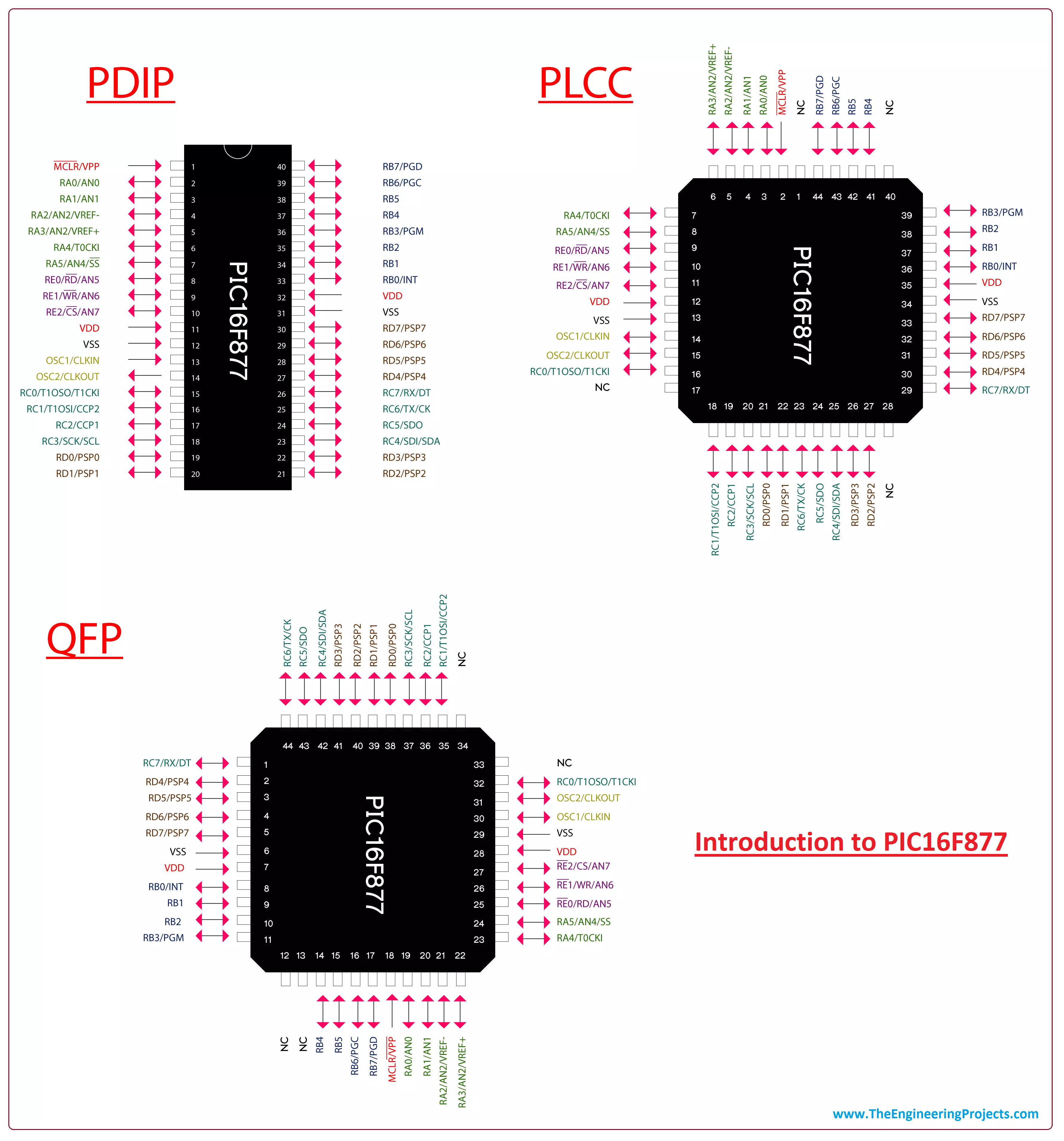
In this section, we cover the pinout of the controller and a detailed description of each pin.PIC16F877 Pinout
Following figure shows the pinout of PIC16F877.
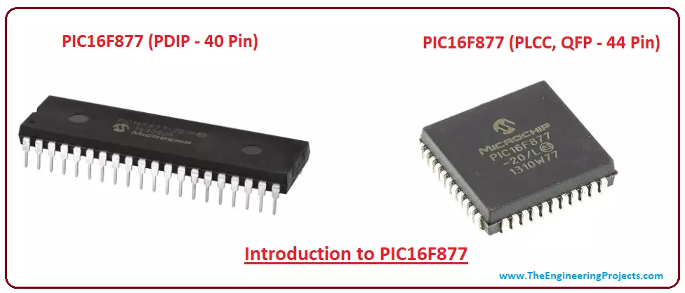
- This module comes in three packages known as PDIP, PLCC, and QFP. The first one is mainly used for developing individual projects while other two are widely used in industrial applications.
PIC16F877 Pin Description
Following table shows the pin description of each pin. Some pins are capable to perform more than one function.| Pin# | Pin Name | Pin Description |
|---|---|---|
| 1 | MCLR' VPP | Master Clear Active Low Reset Pin ICSP Programming Enable Pin |
| 2 | RA0 AN0 | Digital I/O Pin Analog Input 0 Pin |
| 3 | RA1 AN1 | Digital I/O Pin Analog Input 1 Pin |
| 4 | RA2 AN2 VREF- | Digital I/O Pin Analog Input 2 Pin ADC Reference Input Voltage (low) |
| 5 | RA3 AN3 VREF+ | Digital I/O Pin Analog Input 3 Pin ADC Reference Input Voltage (high) |
| 6 | RA4 T0CKI | Digital I/O Pin External clock input for Timer0 |
| 7 | RA5 AN4 SS' | Digital I/O Pin Analog Input 4 Pin Slave Select input for SPI |
| 8 | RE0 AN5 RD' | Digital I/O Pin Analog Input 5 Pin Read control for the parallel slave |
| 9 | RE1 AN6 WR' | Digital I/O Pin Analog Input 6 Pin Write control for the parallel slave |
| 10 | RE2 AN7 CS' | Digital I/O Pin Analog Input 7 Pin Select control for the parallel slave |
| 11 | VDD | Voltage Supply Pin |
| 12 | VSS | Ground Pin |
| 13 | OSC1 CLKIN | Crystal Oscillator Input Pin |
| 14 | OSC2 CLKOUT | Crystal Oscillator Output Pin |
| 15 | RC0 T1OSO T1CKI | Digital I/O Pin Oscillator output for Timer1 External clock input for Timer1 |
| 16 | RC1 T1OSI CCP2 | Digital I/O Pin Oscillator input for Timer1 Output for Compare2 and PWM2, Input for Capture2 |
| 17 | RC2 CCP1 | Digital I/O Pin Output for Compare1 and PWM1, Input for Capture1 |
| 18 | RC3 SCK SCL | Digital I/O Pin SPI Module Synchronous serial clock input/output I2C Module Synchronous serial clock input/output |
| 19 | RD0 PSP0 | Digital I/O Pin Parallel Slave Port for D0 with TTL input buffers |
| 20 | RD1 PSP1 | Digital I/O Pin Parallel Slave Port for D1 with TTL input buffers |
| 21 | RD2 PSP2 | Digital I/O Pin Parallel Slave Port for D2 with TTL input buffers |
| 22 | RD3 PSP3 | Digital I/O Pin Parallel Slave Port for D3 with TTL input buffers |
| 23 | RC4 SDI SDA | Digital I/O Pin SPI Data-In Pin I2C Data I/O Pin |
| 24 | RC5 SDO | Digital I/O Pin SPI Data-Out Pin |
| 25 | RC6 TX CK | Digital I/O Pin Asynchronous Transmit (USART) Synchronous Clock (USART) |
| 26 | RC7 RX DT | Digital I/O Pin Asynchronous Receive (USART) Synchronous Data (USART) |
| 27 | RD4 PSP4 | Digital I/O Pin Parallel Slave Port for D4 with TTL input buffers |
| 28 | RD5 PSP5 | Digital I/O Pin Parallel Slave Port for D5 with TTL input buffers |
| 29 | RD6 PSP6 | Digital I/O Pin Parallel Slave Port for D6 with TTL input buffers |
| 30 | RD7 PSP7 | Digital I/O Pin Parallel Slave Port for D7 with TTL input buffers |
| 31 | VSS | Ground Pin |
| 32 | VDD | Voltage Supply Pin |
| 33 | RB0 INT | Digital I/O Pin External Interrupt 0 |
| 34 | RB1 | Digital I/O |
| 35 | RB2 | Digital I/O |
| 36 | RB3 PGM | Digital I/O ICSP programming enable pin (Low voltage) |
| 37 | RB4 | Digital I/O |
| 38 | RB5 | Digital I/O |
| 39 | RB6 PGC | Digital I/O ICSP programming clock, In-circuit debugger |
| 40 | RB7 PGD | Digital I/O ICSP programming data, In-circuit debugger |
3. PIC16F877 Main Functions
This PIC model is capable to perform many functions similar to other controllers in the PIC family. Following are the main functions of PIC16F877.Timer
PIC16F877 comes with three timers known as Timer0 (8-bit), Timer1(16-bit) and Timer2 (8-bit). These timers can be used as a timer as well as a counter.- The timer mode is mainly used to increment the instruction cycle while the counter mode plays a vital role to increment the rising and falling edge of the pin.
USART
PIC16F877 incorporates a USART (Universal Synchronous and Asynchronous Receiver and Transmitter) module that is mainly used to establish the serial communication with external devices.- This module involves two pins known as TX and RX where former is used for transmitting serial data while later is used for receiving the serial data across the attached devices.
Watchdog Timer
PIC16F877 comes with a built-in watchdog timer that takes the controller back to reset position if the program hangs up during compilation or gets stuck in the infinite loop.- It is nothing but a hardware timer that produces a system reset if the main program fails to periodically service it.
- The Watchdog Timer can be controlled only through configuration bits. It comes with its own RC oscillator for maximum reliability.
Brown Out Reset (BOR)
The BOR function is a very remarkable addition that puts the device in reset condition once the Vdd (voltage supply) drops below a brownout threshold voltage.- If the Power Up Timer is kept enabled, it will create the delay for returning the device from a BOR function. The BOR mode can be configured both ways: BOREN settings in a register or using programming.
In-Circuit Serial Programming
In-circuit serial programming (ICSP), also called In-system programming (ISP), is a function that allows the chip to be programmed in the required project after installation, setting you free from plugging and unplugging the device in the project over and over again.Master Clear Reset (MCLR)
The MCLR pin serves as an external reset for the chip. This pin is independent of the internal resets and is activated by keeping this pin at a LOW value.- The MCLRE configuration bit is mainly used to disable MCLR input and the noise filter is included in the MCLR executing process that allows to detect and remove the small pulses.
Power On Reset
Power On Reset function is a very useful function that resets the controller and prevents it from malfunctioning. When the module is powered on, the power-on reset will start the module from scratch once the Vdd raises above a certain threshold value.- The Power Control (PCON) Register comes with flag bits that help to differentiate between a Power-on Reset (POR), a Watchdog Reset(WDT) and external MCLR Reset.
SPI Communication
Serial Peripheral Interface (SPI) is a remarkable function of the chip that is commonly used to send data between microcontrollers and small peripherals such as sensors, shift registers, and SD cards.
- It comes with separate clock and data lines, layered with a select line to choose the device for communication.
I2C Communication
The I2C is a two-wire interface communication that comes with two main lines known as SDA and SCL where former is s serial data line that carries the data and later is serial clock line that is used to synchronize all data transfers over the I2C bus.4. PIC Compiler
- PIC compilers and burners are used for different purpose. The former is a software used to write the desired code for the module while later is used to transfer and burn the code on the module.
- MikroC Pro For PIC is a third party software and is a good replacement for PIC standard compiler.
- These Top 3 PIC C Compilers give you the flexibility to choose from and pick any compiler as per your needs and demands.
- The PICKit3 is a standard PIC burner for PIC controllers. Other burners are also available in the market but PICKit3 is mostly preferred for the PIC controllers.
5. PIC16F877 Memory Layout and Working
Memory, as the word suggests, is used to store a number of instructions inside the controller. It is mainly divided into three major types: Program Memory (Flash Memory) Data EEPROM Data RAM Let’s get down to the main features of each memory.Program Memory
The Program memory, also known as ROM memory or Flash memory, stores the number of instructions permanently.- It comes with a memory space around 14K and is independent of the power supply i.e. have the ability to store information in the absence of main power supply.
Data EEPROM
The EEPROM Data Memory is similar to ROM memory with one exception i.e. the instructions in EEPROM can be controlled and modified during the controller operation.- The EEPROM incorporates memory space around 256 bytes and is mainly addressed by multiple control registers.
Data RAM
RAM memory, also known as volatile memory, stores the program temporarily and is dependent on the power supply. It comes with a memory space around 368 bytes and is mainly classified into two main parts called General-purpose registers (GPR) Special-function registers (SFR)- These registers are spread across the multiple banks and are the data holding places that can hold instruction, storage address, and any kind of data ranging from an individual character to bit sequence.
- On the other hand, Special function registers are located on the lower side of the banks and are used to control the peripheral functions, covering the first 32 locations of each bank.
6. PIC16F877 Block Diagram
The following figure shows the block diagram of PIC16F877.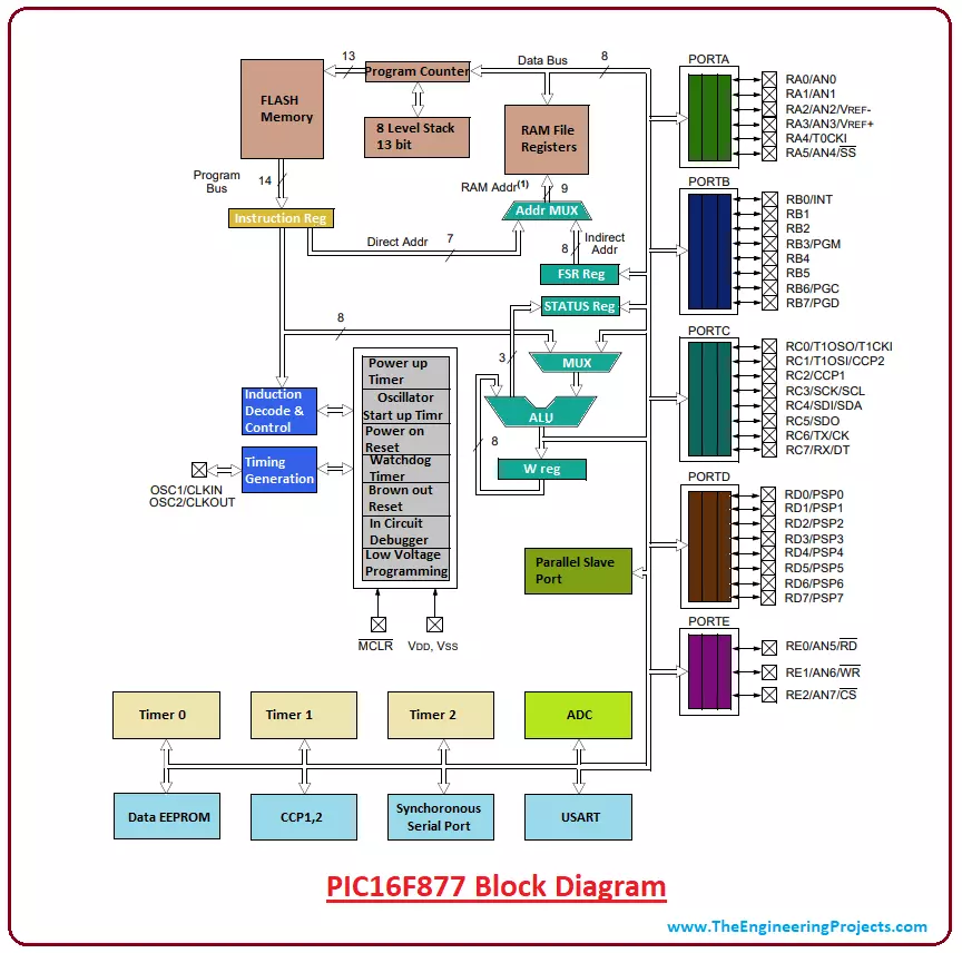
- PIC16F877 comes with five ports where each port contains 8 pins except the E port that comes with 3 pins.
- It is important to note that higher order bits are related to the STATUS register
7. PIC16F877 Projects and Applications
PIC16F877 comes with a variety of applications with the main aim to drive automation in the relevant project. Following are some major applications it can be used for.- Student projects for motor controlling and sensor interfacing
- Health and security systems
- Central heating projects
- Embedded system
- Gas sensor projects
- GPS projects
- Serial Communication
- It is widely used in home and industrial automation
- Production of temperature data logger
8. Why Use PIC MicroControllers
- Earlier, if you were aiming to design the automation project, you'd need a bunch of wires and a plethora of electrical components, that would not only cost you more but making your project heavy with more space requirement. These PIC controllers prove to be a lifesaver for your technical needs requiring minimum circuitry.
- These controllers come with a user-friendly interface and easy onboard architecture that requires little or no prior skills before getting familiar with the chip.
- PIC controllers have a leg over other Atmel controller like 8051 due to their higher processing speed and efficiency.
- They are very handy in terms of consuming minimum power consumption that makes this controller an ideal choice for the projects where power limitation is a major concern.
×
![]()