Hey Guys! Hope you are doing well. This is a platform where we keep you updated with valuable information so you keep coming back for what we have to offer. Today, I'll uncover the details on the Introduction to PIC16F887. It is a 40-pin PIC microcontroller, introduced by Microchip, and is a successor of PIC16F877A.
Microcontrollers have revitalized the technology by providing a flawless interface and an ability to perform numbers of functions on a single chip. Gone are days, when you had to rely on external components to develop your projects which might be time-consuming, covered more space, and required a number of prior skills before making your project in real time. Microcontrollers have made things easy by covering each and every aspect of the projects that are directly or remotely related to automation.
In this tutorial, I'll discuss each and everything related to PIC16F887 including its main features, working, pinout and applications. Let's jump right in and nail down everything you need to know.
Introduction to PIC16F887
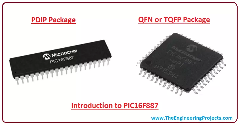
PIC16F887 is a 40-pin (for PDIP package) and 8-bit CMOS PIC Microcontroller that comes with nanoWatt technology. Economical price and user-friendly architecture make this device easy to use and easy to configure.
It is available in three packages known as PDIP, QFN, and TQFP. The first one comes with a 40-pin layout design while remaining two contains 44 pins on each layout.
This PIC version, like other models in the PIC community, contains everything that is required to make an embedded system and drive automation.
The PIC16F887 incorporates 256 bytes of EEPROM data memory, 368 bytes of RAM, and program memory of 8K.
Apart from self-programming capability, it also contains 2 Comparators,10-bit Analog-to-Digital (A/D) converter with 14 channels, and capture, compare and PWM functions.
The asynchronous serial port is added on the chip that can be configured both ways i.e. the 2-wire Inter-Integrated Circuit (I²C™) Bus or 3-wire Serial Peripheral Interface (SPI™)
The Enhanced Universal Asynchronous Receiver Transmitter (EUSART) feature makes this chip compatible with the devices where serial communication is an integral part of the project.
The functions that make this device unique in terms of ease of use include
Power-Saving Sleep mode
Industrial and Extended Temperature range
Wide operating voltage range (2.0V-5.5V)
SR Latch mode
Power-up Timer (PWRT) and Oscillator Start-up Timer (OST)
Power-on Reset (POR)
Ultra-Low-Power Wake-up (ULPWU)
Multiplexed Master Clear with pull-up/input pin
Individually programmable weak pull-ups
Brown-out Reset (BOR) with software control option
Enhanced low-current Watchdog Timer (WDT)
Needless to say, this PIC version is an ideal choice to drive A/D conversion in automotive, consumer, and industrial applications.
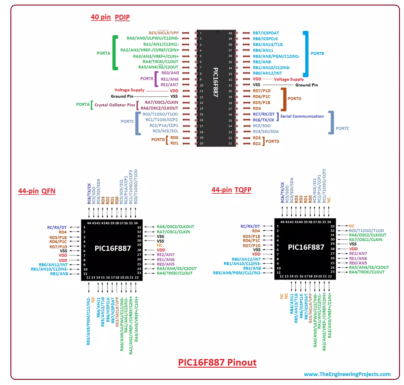
1. PIC16F887 Pinout & Description
Getting a hold of Pinout and Pin descriptions is mandatory to check the working of each pin on this tiny chip. If you are a newbie or an expert, you need to know the function associated with each pin for a better understanding of the chip.
Pinout
The following figure shows the complete pinout of all three packages called PDIP, QFN, and TQFP.
As described earlier, the PDIP package contains 40-pin while other two come with 44 pins.
Pin Description
PIC16F887 is widely used in many electronic applications. Some pins in the controller are capable of doing more than one functions that allow us to use the pin according to the needs and demands of the project.
I have listed the function of each pin in the following table.
Pin#
Pin Name
Pin Description
2
RA0
AN0/ULPWU
C12IN0-
Digital I/O Pin
Analog Input 0 Pin
Comparator
3
RA1
AN1/ULPWU
C12IN1-
Digital I/O Pin
Analog Input 1 Pin
Comparator
4
RA2
AN2
C2IN+
VREF-/CVREF
Digital I/O Pin
Analog Input 2 Pin
Comparator
ADC Reference Input Voltage (low)
5
RA3
AN3
C1IN+
VREF+
Digital I/O Pin
Analog Input 3 Pin
Comparator
ADC Reference Input Voltage (high)
6
RA4
C1OUT
T0CKI
Digital I/O Pin
Comparator
External clock input for Timer0
7
RA5
AN4
C2OUT
SS
Digital I/O Pin
Analog Input 4 Pin
Comparator
Slave Select input for SPI
33
RB0
AN12
IOC/INT
Digital I/O Pin
Analog Pin
Interrupt-on-change
34
RB1
AN10
C12IN3-
IOC
Digital I/O Pin
Analog Pin
Comparator
Interrupt-on-change
35
RB2
AN8
IOC
Digital I/O Pin
Analog Pin
Interrupt-on-change
36
RB3
AN9
C12IN2-
IOC
PGM
Digital I/O Pin
Analog Pin
Comparator
Interrupt-on-change
Basic
37
RB4
AN11
IOC
Digital I/O Pin
Analog Pin
Interrupt-on-change
38
RB5
AN13
T1G
IOC
Digital I/O Pin
Analog Pin
Timer
Interrupt-on-change
39
RB6
IOC
ICSPCLK
Digital I/O Pin
Interrupt-on-change pin
Basic
40
RB7
IOC
ICSPDAT
Digital I/O Pin
Interrupt-on-change pin
Basic
15
RC0
T1OSO/T1CKI
Digital I/O Pin
Timer
16
RC1
T1OSI
CCP2
Digital I/O Pin
Timer
ECCP
17
RC2
CCP1/P1A
Digital I/O Pin
ECCP
18
RC3
SCK/SCL
Digital I/O Pin
MSSP
23
RC5/SDO
RC5
SDO
Digital I/O Pin
SPI Data-Out Pin
24
RC5
SD0
Digital I/O Pin
MSSP
25
RC6
TX/CK
Digital I/O Pin
USART
26
RC7
RX/DT
Digital I/O Pin
USART
19
RD0
Digital I/O Pin
20
RD1
Digital I/O Pin
21
RD2
Digital I/O Pin
22
RD3
Digital I/O Pin
27
RD4
Digital I/O Pin
28
RD5
P1B
Digital I/O Pin
ECCP
29
RD6
P1C
Digital I/O Pin
ECCP
30
RD7
P1D
Digital I/O Pin
ECCP
8
RE0
AN5
Digital I/O Pin
Analog Pin
9
RE1
AN6
Digital I/O Pin
Analog Pin
10
RE2
AN7
Digital I/O Pin
Analog Pin
13
RA7
OSC1
CLKIN
Crystal Oscillator Input Pin
14
RA6
OSC2
CLKOUT
Crystal Oscillator Output Pin
1
RE3
MCLR
VPP
ICSP Programming Enable Pin
Master Clear Active Low Reset Pin
11,32
VDD
Voltage Supply Pin
12,31
VSS
Ground Pin
2. PIC16F887 Features
You can anticipate the nature of any device by looking at its main features. Following table shows the complete features of PIC16F887.
PIC16F887 Features
No. of Pins
40
CPU
8-Bit PIC
Operating Voltage
2 to 5.5 V
Program Memory
8K
Program Memory (Instructions)
8192
RAM
368 Bytes
EEPROM
256 Bytes
ADC
10-Bit
I/O Ports (5)
I/O Pins
A,B,C,D,E
35
Packages
40-pin PDIP
44-pin QFN
44-pin TQFP
External Oscillator
up to 20 MHz
Timer (3)
16-Bit Timer (1)
8-Bit Timer (2)
USART Protocol
1
I2C Protocol
Yes
SPI Protocol
Yes
Brown-out Reset
Yes
Watchdog Timer
Yes
Comparators
2
Master Synchronous Serial Port (MSSP) module
1
Capture/Compare/PWM
16bit/16bit/10bit
Power Saving Sleep Mode
Yes
Selectable Oscillator Option
Yes
Operating Current
11uA at 32 kHz, 2.0 V
220uA at 4 MHz, 2.0 V
Temperature Range
-40 to 125
Oscillator Start-up Timer
Yes
Checking main features before purchasing of the controller will help you analyze and develop your required project.
Power on reset and selectable oscillator options are some unique features included in the chip.
3. PIC16F887 Functions
This PIC model performs many functions that are quite similar to the function in other controllers of the PIC community. Following are the main functions of PIC16F887.
Timer
PIC16F887 contains one 16-bit timer and two 8-bit timers that can be used in both ways i.e. timer and counter and comes with internal and external clock select capability.
The timer mode is used to increment the instruction cycle while counter mode increments the rising and falling edge of the pin.
When the bit T0CS (OPTION_REG<5>) is set, the counter mode will be selected and when it is cleared, the timer mode will be selected.
Brown Out Reset (BOR)
The BOR is a function that brings the controller to reset once the Vdd (voltage supply) drops below a brownout threshold voltage. There is a fine line between a BOR and Power On Reset, where the whole range of voltages is provided to protect the chip once the power drops at the voltage supply line.
In order to put the delay, mostly recommended, in returning from a BOR function, the Power Up Timer must be kept enabled.
Apart from controlling through software, the BOR mode can also be handled and configured through BOREN settings in a register.
USART
PIC16F887 comes with enhanced USART module.
This module consists of TX - A transmission pin used for transmitting serial data to other devices and RX - A receive pin used for receiving serial data.
Watchdog Timer
PIC16F887 comes with built-in watchdog timer that is mainly used to reset the controller when a program hangs up during compilation or gets stuck in the infinite loop of the program.
It is important to note the timer must be reset to the initial value after every 3 instructions in order to avoid it going to zero value in normal conditions.
The watchdog timer is nothing but a countdown timer and starts from 1000 and gradually goes down to zero.
Power On Reset
Power On Reset function resets the controller when it is powered on. If there comes unknown error in the chip, powering on the device will exclude it from the loop of running program and saves the device from malfunctioning.
Sleep Mode
Power saving sleep function generates a low current power down mode. This sleep mode can be terminated using an interrupt, watchdog timer or external reset.
4. PIC Compiler
Microchip has introduced its own standard compiler for the PIC controller called MPLAB C18 Compiler. You can download this compiler online from the Microchip Official Site.
The code written in the compiler creates a hex file that is transferred to the microcontroller to execute the certain function.
Third party softwares are also available for compiling the program and MikroC Pro For PIC is mainly used for this purpose.
These Top 3 PIC C Compilers give you the flexibility to pick any compiler based on your needs and requirements.
The PICKit3 is mainly used for burning the code in the controller which is a standard PIC burner. There are other unofficial burners also available but PICKit3 is mostly preferred for the PIC controllers.
5. PIC16F887 Memory Layout and Working
The whole memory in this controller is distributed into three main types known as EEPROM, RAM and ROM Memory. All of them plays a vital role in the controller in terms of executing and calling instructions with some exceptions. Let's discuss each of them one by one.
ROM Memory
ROM memory, also known as Non-Volatile memory, which stores the running program permanently and is not dependent on the power supply i.e. has an ability to retain the program if the power supply is removed. The ROM memory is about 8K made with FLASH Technology.
EEPROM Memory
This memory is quite similar to ROM memory in one way or the other in terms of storing running program permanently with the exception i.e. the instructions in EEPROM can be modified during the operation of the controller. It contains memory space around 256 bytes, quite less than ROM memory, but enough to store the program permanently.
RAM Memory
RAM memory, also known as volatile memory, is divided into two main parts known as general-purpose registers (GPR) and special-function registers (SFR). This memory is volatile in nature as it stores the program temporarily and is power dependent i.e. once the power supply is turned off the instructions stored in the RAM will be removed.
Registers in the RAM memory are the data holding places in the controller. A single register can hold instruction, storage address, and any kind of data including bit sequence or individual characters.
Registers are classified into two banks called Bank 1 and Bank 2 where registers from 00H to 0BH and 80H to 8BH fall under the category of SFRs and remaining are GPRs.
Each bank contains128 bytes of memory space where first 12 locations are reserved for SFR while remaining are reserved for GPR.
Let’s discuss few registers in details.
STATUS. This register plays a role to switch between the banks. Setting fifth bit of this register shows we are discussing bank 1 while resetting it will indicate we are discussing bank 0.
TRISA. This register is used to configure PORTA as an input or output. The value 1 shows output and value 0 shows input.
TRISB. This register is identical to the TRISA in terms of deciding the pins as an input or output and used for PORTB.
W Register. All registers mentioned above are SFRs while W register is a GPR. It is not a part of any register bank and is accessible by the program only. The desired values are written on W register and transferred to the target register before writing them on the PORTA or PORTB.
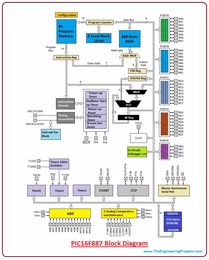
6. PIC16F887 Block Diagram
The following figure shows the block diagram of PIC16F887.
The program memory comes with 8K memory space which can configure 8192 words.
Some pins can be interfaced with other functions of multiple devices including external interrupt, Timer0 clock input and Change on PORTB interrupt.
7. PIC16F887 Projects and Applications
PIC16F887 is mainly used in students project i.e. controlling motors and sensor interfacing.
PIC microcontrollers are widely used in most of the electronic applications because they offer easy to use interface that requires no prior skills for getting a hands-on experience with the module.
These controllers are cheap and come with an ability to perform a number of functions using minimum circuitry.
PIC controllers have outperformed Atmel controller like 8051 in terms of their efficiency and higher processing speed.
More often than not, automation industries prefer and use these controllers for carrying out different operations as they offer very little power consumption.
That’s all for today. I hope I have given you everything related to PIC16F887. If you are unsure or have any query, you can ask me in the comment section below. I’d love to help you in any way I can. You are most welcome to give your feedback and suggestions, they help us provide you quality work as per your needs and demands. Thanks for reading the article.