


LM3914 PCB Footprint
 Libraries
 Code
 Projects
 Simulation
TEP_TI-PLCC20-FN.kicad_mod
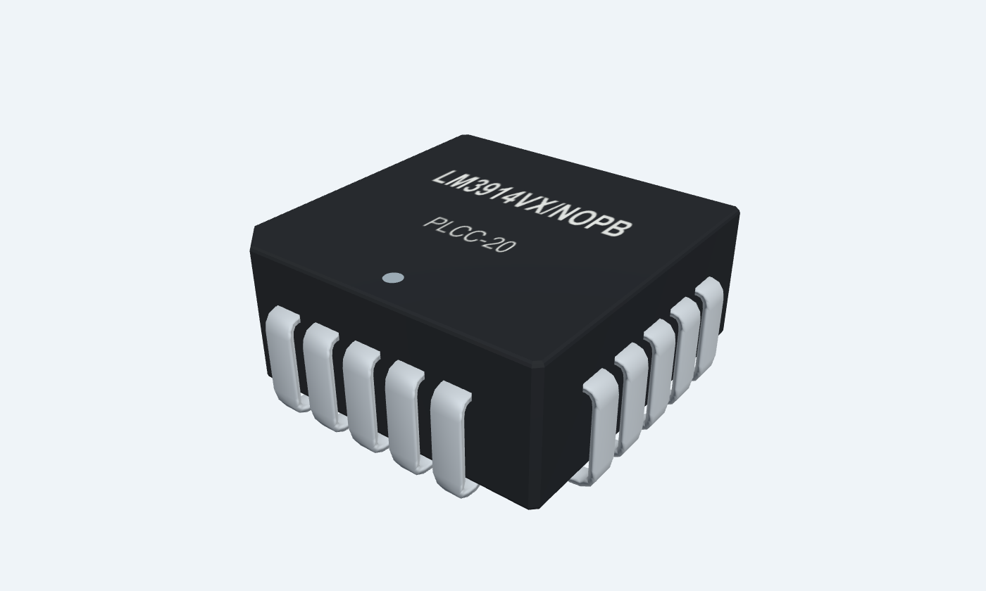
TI-PLCC20-FN KiCad PCB Footprint
LM3914 · LM3914VX/NOPB · PLCC-20: an editable KiCad footprint with 20 numbered pads at 1.27 mm pitch.
- PCBPCB / schematic
Description
Editable KiCad footprint with numbered copper pads, drill dimensions and package outlines.
Use in KiCad
- Download the .kicad_mod file.
- Create a folder named TEP.pretty and put the file inside.
- In KiCad, open Preferences → Manage Footprint Libraries and add that folder.
- Select the footprint in the Footprint Editor or assign it to your schematic symbol.
Dimensions are in millimeters. Confirm the package and pin mapping against your chosen part before fabrication. This is a footprint, not a complete PCB or 3D model.

File Structure
 File Structure

Installation4 steps
 Installation4 steps
From the download to a working project, in order. The steps follow what the package contains.
You will need
- KiCadAdd the .kicad_mod file to a .pretty footprint library.
Steps
- 1
Create a footprint library
Create a folder named TEP.pretty and put the downloaded .kicad_mod file inside.
- 2
Add it to KiCad
Open Preferences → Manage Footprint Libraries and add the TEP.pretty folder. Open the footprint in the Footprint Editor or assign it to a schematic symbol.
- 3
Check your chosen package
Verify the pin mapping, pad dimensions and drill sizes against your component before fabricating the PCB. Dimensions are in millimeters.
- 4
Check the component datasheet
Use the LM3914 package drawing and pinout to confirm pad numbers and dimensions before manufacturing.
FAQs5 questionsContact TEP
 FAQs5 questions
How do I download the LM3914 footprint?
Select the matching package, wait for the countdown and press Download. Guests wait 30 seconds and signed-in members wait 10 seconds.
What if the download does not start?
Check your browser's downloads, then try the button again. Expired links renew automatically. For help, use Bug report below and include your browser and KiCad version.
Which package should I choose?
This selection is LM3914VX/NOPB in PLCC-20. Match your actual component's package and pad numbering; through-hole and surface-mount footprints are not interchangeable.
Does this include a complete PCB or 3D model?
This .kicad_mod file is an editable footprint. The interactive datasheet separately provides schematic, pinout and 3D previews.
How can I verify the file?
Compare its SHA-256 against the checksum on this page. In PowerShell run Get-FileHash TEP_TI-PLCC20-FN.kicad_mod.
Members skip the wait. Log in or join TEP.

- PLCC-20Package
- SMD · obsolete orderableMounting
- 20Pads
- 1.27 mmPin pitch
- KiCad footprintFormat
- 3 KBSize

 SHA-256
32d0747f739eaa6f8f03c1f49f6f39aab66c5ec5c626ce9e5ce414e727bac111

 Need help with this file?
 Ask a question
 Get updates