LM747 Datasheet, Pinout, Features, Equivalent & Applications

Hi Guys! I hope you’re well today. Happy to see you around. In this post today, I’ll walk you through the Introduction to LM747.

LM747 is a general-purpose dual-operational amplifier IC. This chip contains two operational amplifiers on board and belongs to the LM’xx’ family where LM stands for linear monolithic. In this chip, analog components are incorporated into silicon.

I suggest you buckle up as I’ll detail the complete Introduction to LM747 covering datasheet, pinout, features, equivalents, and applications. Let’s jump right in.

Introduction to LM747

  • Designed by National Semiconductor, LM747 is a general-purpose dual-operational amplifier integrated chip.
  • Two operational amplifiers are incorporated that share common power supply leads and a bias network.

  • And these amplifiers are capable of performing two different operations at the same time which makes them a suitable pick for several applications. Though these amplifiers share a common bias network, they are completely independent of each other
  • As two general-purpose amplifiers are used in this chip, it is used to construct op-amp circuits like differential amplification, comparator, and mathematical operations.
  • This device features offset pins which are mainly used to make the output more accurate and efficient.
  • It comes with no latch-up when the input common-mode range is exceeded which sets it free from oscillations.

LM747 Datasheet

Before you incorporate this device into your electrical project, it’s better to scan through the datasheet of the component that features the main characteristics of the component. You can download the datasheet of LM747 from the link given below.

LM747 Pinout

LM747 incorporates 14 pins on board. The following figure shows the pinout diagram of LM747. The following table details the pin name and pin description of each pin on LM747.
Pin Description of JRC4558
Pin No. Pin Description Pin Name
1 Inverting input of op-amp 1 1IN-
2 A non-inverting input of op-amp 1 1IN+
3 The offset null pin is used to remove the offset voltage and control the input voltages for op-amp 1 OFFSET  NULL 1
4 Common negative supply voltage for both Op-amps V-
5 The offset null pin is used to remove the offset voltage and control the input voltages for op-amp 1 OFFSET  NULL 2
6 The non-inverting input of op-amp 2 2IN+
7 Inverting  input of op-amp 2 2IN-
8 The offset null pin is used to remove the offset voltage and control the input voltages for the op-amp 2 OFFSET  NULL 2
9 Positive supply voltage for op-amp 2 V2+
10 The output pin of the op-amp 2 2OUT
11 No connection NC
12 The output pin of the op-amp 1 1OUT
13 Positive supply voltage for op-amp1 V1+
14  The offset null pin is used to remove the offset voltage and control the input voltages for op-amp 1 OFFSET  NULL 1
  • Offset null pins remove the offset voltage and balance the output voltages for both operational amplifiers.
  • While pin 11 is not connected. It is not used for any purpose.

LM747 Features

The following are the main features of LM747.
  • No latch-up
  • Large differential voltage and common mode range
  • Low noise interference among op-amps
  • Total power dissipation = 800mW
  • Differential input voltage = ±30V
  • Low power consumption
  • Supply voltage Max. = ±22V
  • Frequency Compensation is not required
  • Comes with short-circuit protection
  • Common-Mode Rejection Ratio CMRR = 90dB
  • Operating temperature range = -55ºC to +125ºC

LM747 Applications

The following are the main applications of LM747.
  • Employed in mathematical operations
  • Used in amplifiers
  • Used in analog circuits
  • Used for Measuring instruments
  • Incorporated in voltage comparators
  • Employed for Industrial applications
  • Used in Peak detectors

That was all about the Introduction to LM747. If you’re unsure or have any questions, you can leave your query in the section below. I’d love to help you according to the best of my expertise. Feel free to share your valuable feedback and suggestions around the content we share so we keep sharing quality content tailored to your exact needs and requirements. Thank you for reading the article.

LF353N Dual JFET Input Op-Amp Datasheet, Pinout, Features & Applications

Hi Folks! I hope you’re well today. I welcome you on board. Happy to see you around. In this post today, I’ll walk you through the Introduction to LF353N.

The LM393N is a wide bandwidth and high input impedance Dual Input JEFET op-amp that is widely used in high-speed integrators and low noise circuits. The low bias current and input noise make it a good pick for audio amplifier applications. It carries a high slew rate (13V/uS) and wide bandwidth around (4MHz).

I suggest you read this post all the way through, as I’ll detail the complete introduction to LF353N covering datasheet, pinout, features, and applications. Let’s dive in.

Introduction to LF353N

  • Introduced by the Texas Instrument, the LM393N is a high input impedance dual op-amp where the input of this device is attached through a high voltage JFET.
  • It is widely used in low current, low noise fast switching applications.

  • There are two outputs available on the device i.e. Output A and Output B. And two inputs where each input contains further two inputs i.e. inverting input (-) and non-inverting input (+).
  • This chip incorporates two independent op-amps that operate over a wide range of voltages from a single power supply.
  • High slew rate and high input impedance device, LF353N comes with internally compensated input offset voltage.
  • It is also available with a power supply voltage range of ±18 V and with a differential input voltage of around 30V.
  • The power dissipation Pd is 500mW which is defined as the maximum energy dissipated during the working of this device.

LF353N Datasheet

Before you incorporate this device into your electrical project, it’s wise to scan through the datasheet of the component that features the main characteristics of the component. Click the link below to download the datasheet of LF353N.

LF353N Pinout

The following figure shows the pinout diagram of LF353N. This chip incorporates total 8 pins on board. The following table shows the pin name and pin description of each pin installed on the device.
Pin Description of LF353N
Pin No. Pin Description Pin Name
1 The output of Op-Amp 1 OUT (A)
2 Inverting Input of Op-Amp 1 INPUT- A(-)
3 Non-Inverting Input of Op-Amp 1 INPUT- A(+)
4 Ground or Negative supply terminal Power (-Vs)
5 Non-Inverting Input of Op-Amp 2 INPUT- B(+)
6 Inverting Input of Op-Amp 2 INPUT- B(-)
7 The output of Op-Amp 2 OUTPUT B
8 Positive supply terminal +Vcc

LF353N Features

  • Dual Op-Amp that comes with JFET Input
  • High slew rate 13V/µs
  • High Input Impedance 1012?
  • Low Input Noise current
  • Low input noise voltage
  • Supply Current = 6.5mA (max)
  • Bandwidth Gain = 4MHz
  • Supply Voltage = ±18V
  • Available Packages = 8-pin SOIC & PDIP Package

LF353N Equivalent

The following are the equivalents of LF353N.
  • LM1558
  • TL074
  • MCP6002

While working with the alternatives, make sure you cross-check the pinout of them. It’s quite likely the pinout of the alternatives might differ from the pinout of LF353N.

LF353N Applications

The LF353N is used in the following applications.

  • Used in High-Input Impedance designs
  • Employed in Low-noise Audio circuits
  • Used in High-Speed Integrator
  • Incorporated in Sample and Hold Circuit

That’s all for today. I hope you’ve loved reading this article. If you have any questions, you can approach me in the section below, I’d reply to you according to the best of my experience. Feel free to share your valuable suggestions and feedback around the content we share, so we keep producing quality content customized to your needs and requirements. Thank you for reading this article.

MID400 Optocoupler Datasheet, Pinout, Features, Equivalent & Applications

Hi Everyone! I hope you’re well today. Happy to see you around. In this post today, I’ll walk you through the Introduction to MID400.

The MID400 is an 8-pin optically isolated AC line-to-logic Power Line Monitor Optocoupler. The AC line voltage is detected by two back-to-back LEDs that are connected in series with an external resistor. When this device identifies the AC voltage, the output pin goes low and when there is no AC voltage detected, it remains high.

This feature of detecting the AC line voltage is widely employed in AC to DC control and relay latching applications. I suggest you buckle up as I’ll walk you through the complete introduction to MID400 covering datasheet, pinout, features, equivalents, and applications. Let’s dive right in.

Introduction to MID400

  • The MID400 is an 8-pin optically isolated AC line-to-logic Power Line Monitor Optocoupler that identifies the AC line voltage using two back-to-back LEDs that are attached in series with an external resistor.

  • It features high voltage isolation between input and output and comes with an externally adjustable AC voltage sensing level.
  • This device is available with an 8-pin compact DIP package and SMD Package.
  • It is the best pick for AC to DC control applications where remarkable solid-state reliability and excellent optical isolation are needed.
  • It is also applied to low-frequency operations where small size, low power, and TTL compatibility are required.

MID400 Datasheet

While working with this device, it’s wise to go through the datasheet of the component before installing this device into your project. The datasheet highlights the main characteristics of the component. Click the link below if you want to download the datasheet of MID400.

MID400 Pinout

The following figure represents the pinout diagram of MID400.

The following table demonstrates the pin description of MID400.

Pin Description of MID400
Pin No. Pin Description Pin Name
1 AC Live wire is connected to this Pin AC Live
2 No connection Not used
3 AC Neutral wire is connected to this pin AC Neutral
4 No connection Not used
5 The ground pin of the device Ground
6 Open collector output pin V Output
7 Used to control time delay and AC voltage sensing by adding a capacitor to this pin Auxiliary
8 Device Operating Voltage Vcc

You can see from the table above… out of 8 pins, two pins(2 & 4) are not used for any connection. Pin 5 is the ground and Pin 8 is the voltage supply pin.

MID400 Features

The following are the main features of MID400.

  • Working Insulation Voltage Max. = 630Vpeak
  • LED on-state input current = ±30mA
  • Power Line Monitor IC
  • Low-level Output Current = 20mA
  • Low-level Output Voltage = 0.18V
  • LED forward voltage drop = 1.5V
  • Supply Voltage (Vcc) = 7V
  • Turn-on and Turn-off Time = 1ms each
  • Available Packages = 8-pin DIP and SMD Package

MID400 Sample Application Circuit

The following figure shows the sample application circuit of MID400.
  • MID400 is an AC line monitor where the phase wire is connected to the first pin of the device and the neutral wire is connected to the third pin of the device using a resistor of 22-kilo ohm. This resistor is used to control and limit the current flowing through the AC line voltage.
  • Pin 6 is the output pin that remains high when there is no AC voltage and it remains low when AC line voltage is detected.
  • Optocoupling property is used in this device which keeps both output voltage and AC line completely isolated.
  • Pin 6 is the output pin or open collector pin that is attached to the pull-up resistor of 300 ohms which is further connected with the Vcc pin of the device… as shown in the figure above.
  • The capacitor is attached to pin 7 which is mainly used to control the time delay and sensing level of the output.

MID400 Alternative

The following are the alternatives to MID400:

  • ACS71020
  • UC1903

While working with the alternatives, double-check the pinout of the alternatives, as the pinout of the alternatives might differ from the pinout of MID400.

MID400 Applications

MID400 is used in the following applications.

  • Employed in AC sensing applications
  • Employed in Latching circuits
  • Incorporated in Isolation switch
  • Used in AC to DC control applications
  • Used in AC to DC converters

That was all about the Introduction to MID400. If you’re unsure or have any queries, you can pop your question in the section below. I’d love to help you the best way I can. You’re most welcome to share your valuable suggestions and feedback around the content we share, so we keep producing quality content tailored to your exact needs and requirements. Thank you for reading the article.

TDA7265 Audio Amplifier Datasheet, Pinout, Features & Applications

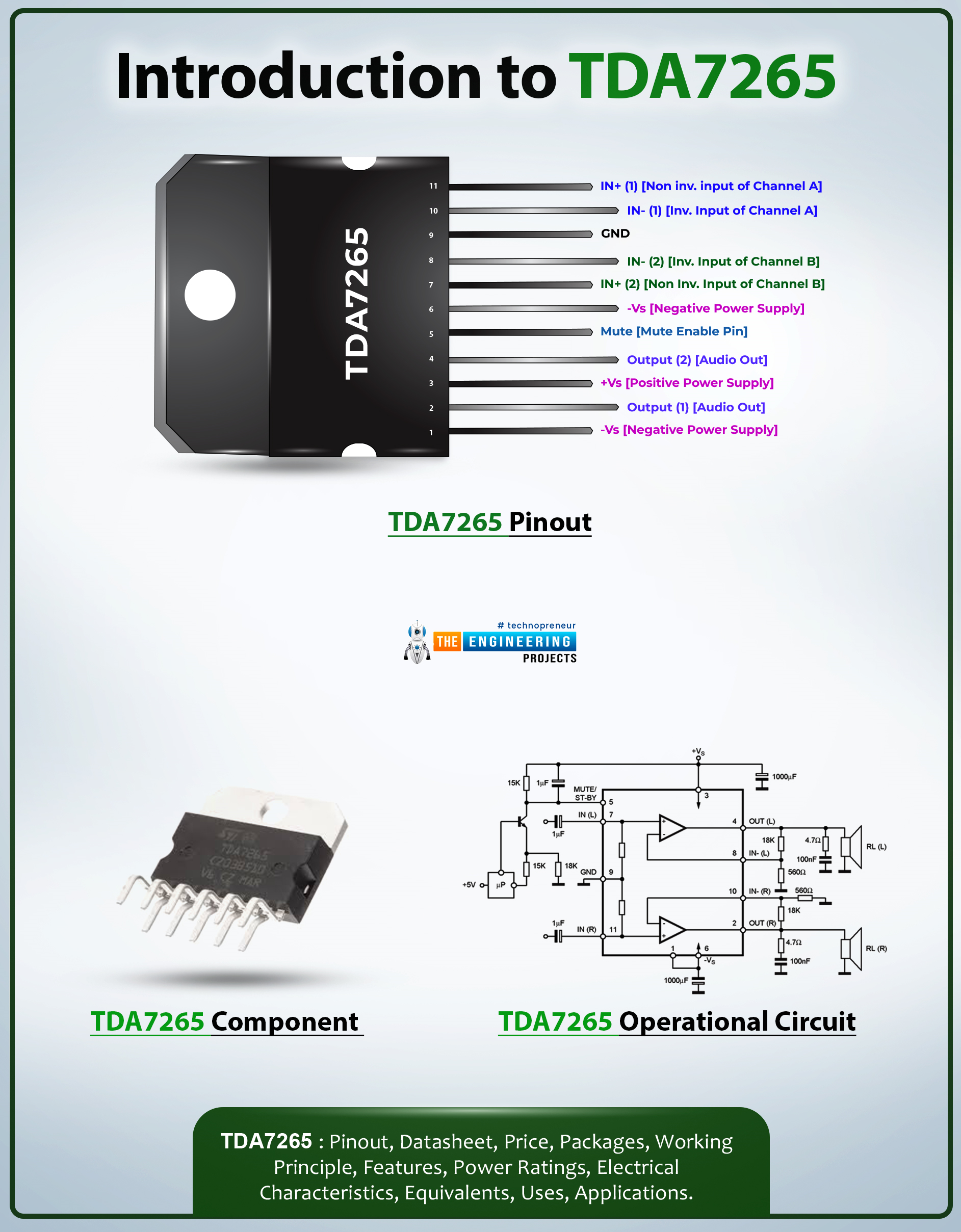
Hi Friends! I hope you’re well today. I welcome you on board. In this post today, I’ll walk you through the Introduction to TDA7265.

TDA7265 is a +25-watt class AB dual audio power stereo amplifier. This multi-watt package IC is carefully designed for high-quality audio power amplification applications. This device receives a low-input audio signal and amplifies it into a high-quality audio output.

I suggest you buckle up as I will detail the complete introduction to TDA7265 covering datasheet, pinout, features, and applications. Let’s jump right in.

Introduction to TDA7265

  • TDA7265 is a +25-watt class AB dual audio power stereo amplifier that is mainly employed in audio amplifiers and woofer amplifiers.
  • This device gets a low-input audio signal and converts it into a high-output audio signal.

  • This chip features output short circuit protection and comes with a mute-enabled pin.
  • Only a few components are required to put this device into working condition.
  • Total power dissipation is 30W which is the amount of energy released during the working of this device.
  • It comes with an operating voltage range of ±5 to ±25V.
  • The operating temperature range is -20°C to +85°C while the storage temperature range is -40°C to +150°C.

TDA7265 Datasheet

Before you apply this component to your electrical project, it’s wise to scan through the datasheet of the device that comes with the main characteristics of the component. Click the link below and download the datasheet of TDA7265.

Additional circuit configurations are available in the datasheet of this chip. You can use any configuration to put this chip in working condition.

TDA7265 Pinout

The TDA7265 incorporates 11 pins on the device. The following figure shows the pinout diagram of TDA7265.

The table below demonstrates the pin name and pin description of each pin on the board.

Pin Description of TDA7265
Pin No. Pin Description Pin Name
1 A negative power supply is connected to this pin -Vs
2 This pin receives the amplified output of channel A OUTPUT 1
3 A positive power supply is connected to this pin +Vs
4 This pin receives the amplified output of channel B OUTPUT 2
5 This pin is triggered low to disable the audio output MUTE
6 A negative power supply is connected to this pin -Vs
7 A non-inverting input of channel B amplifier IN+(2)
8 Inverting input of channel B amplifier IN-(2)
9 This pin is connected to the ground GND
10 Inverting input of channel A amplifier IN-(1)
11 A non-inverting input of channel A amplifier IN+(1)

TDA7265 Features

The following are the main features of TDA7265.

  • Comes with a wide operating supply voltage range
  • Available with High output power : 25 + 25 W @ RL = 8 ?, Vs = ± 20V
  • Features output short circuit protection
  • Comes with a mute enable pin
  • Incorporates thermal overload protection
  • A few components are required to put the amplifier in working condition
  • Stand-by feature (low Iq)
  • Total power dissipation = 30W
  • Split supply
  • Maximum supply voltage = ±25V
  • Operating voltage range = ±5 to ±25V
  • Repetitive current allowed to draw through each output Max = 4.5A
  • Storage Temperature = -40°C  to +150°C
  • Operating temperature = -20°C  to +85°C
  • No pop at turn-on/off

TDA7265 Operational Circuit

The following figure shows the operational circuit diagram of TDA7265. You need to connect the components as shown in the figure below. Doing this will put your amplifier in working condition.

  • Two power supplies are used to power up this circuit one with the negative voltage V- and the other with the positive voltage V+.
  • Pin no. 11 of this chip is given with the audio input signal for channel B and the resulting amplified output is heard through the right speaker. The Pin no. 07 of this chip is given with the audio input signal for channel A and the resulting amplified output is heard through the left speaker.
  • A positive voltage supply source is used to power up the TDA7265 chip while the separate control unit is used to trigger the mute pin low. The two amplified outputs behave as a dual supply operation.

TDA7265 Applications

The TDA7265 is used in the following applications.
  • Employed in stereo TV sets
  • Incorporated in woofer amplifiers
  • Used in audio power amplifiers
  • Used in music players
  • Used in student and hobby projects
  • Employed in guitar amplifiers
  • Used in Hi-Fi music centers

That’s all for today. I hope you’ve enjoyed reading this article. If you’re unsure or have any questions, you can ask me in the section below. I’d love to help you the best way I can. Feel free to share your valuable suggestions and feedback around the content we share, so we keep producing quality content customized to your exact needs and requirements. Thank you for reading the post.

LM4558 Dual Op-Amp Datasheet, Pinout, Features & Applications

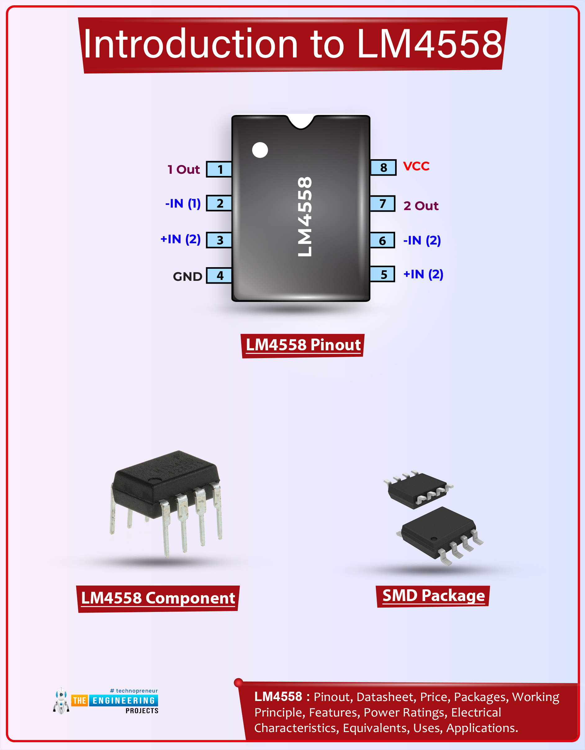
Hi Friends! I welcome you on board. Happy to see you around. In this post today, I’ll walk you through the Introduction to LM4558.

LM4558 is a dual-operational amplifier that comes with two amplifiers on board. This device belongs to the LM’xx’ family where LM stands for linear monolithic which means, it is made of analog components that are incorporated into the silicon piece.

This component comes with an internal frequency compensation method that guarantees the device's stability without the need for external components.

I suggest you read this post all the way through as I’ll detail the complete Introduction to LM4558 covering datasheet, pinout, features, and applications. Continue reading.

Introduction to LM4558

  • LM4558 is a monolithic dual-operational amplifier that carries two amplifiers on board.

  • This device belongs to the LM’xx’ family where LM stands for linear monolithic which demonstrates the availability of analog components that are incorporated on the silicon piece.
  • It comes with a high common-mode input voltage range and no latch-up on this device makes it an ideal pick for voltage-follower applications.
  • This chip comes with an internal frequency compensation method that guarantees the device's stability. Moreover, it is protected against short-circuiting.
  • The device can be utilized in the op-amp operation circuits including differential amplification, comparators, and mathematical operations.
  • As this component exhibits two independent amplifiers on board, it is capable of performing two completely different operations at the same time which makes it a suitable pick for several applications.
  • The LM4558 comes with an operating temperature range from 0ºC to 70ºC while the total power dissipation is 200mW.
  • The common-mode Rejection Ratio CMRR is 80dB and these amplifiers feature low noise interference.

LM4558 Datasheet

While working with this device, it’s wise to go through the datasheet of the component that features the main characteristics of the component. You can download the datasheet of LM4558 by clicking the link below.

LM4558 Pinout

This chip is an 8-pin device. The following figure shows the pinout diagram of LM4558.

The following table represents the pin name and pin description incorporated on the chip.

Pin Description of JRC4558
Pin No. Pin Description Pin Name
1 The output pin of the Op-amp 1 1OUT
2 The inverting input of Op-amp 1 1IN-
3 The non-inverting input of Op-amp 1 1IN+
4 Ground or Negative supply terminal GND
5 A non-inverting input of Op-amp 2 2IN+
6 The inverting input of Op-amp 2 2IN-
7 The output pin of the Op-amp 2 2OUT
8 Positive supply terminal VCC

LM4558 Features and Specifications

The following are the main features and specifications of LM4558.

  • Low noise interference among op-amps
  • Dual  Supply Operation = +15V and -15V
  • No frequency Compensation Required
  • Operating temperature = 0ºC to 70ºC
  • Common-Mode Rejection Ratio CMRR = 80dB
  • Two independent operational amplifiers
  • Built-in Short-Circuit Protection
  • No latch-up
  • Large common mode and differential voltage range
  • Total power dissipation = 200mW
  • Parameter tracking over a temperature range
  • Carries low noise input transistors
  • Phase and gain match between amplifiers
  • Moisture Sensitivity Level 3
  • Single Supply Operation = +5.0 V to +15 V

LM4558 Applications

The LM4558 is used in the following applications.

  • Used in Measuring instruments
  • Employed in Industrial applications
  • Incorporated in Logic voltage translation
  • Used in voltage comparators and peak detectors
  • Employed in oscillators and amplifiers
  • Used in mathematical operations

That’s all for today. I hope you’ve enjoyed reading this article. If you have any questions, you can pop your queries in the section below, I’d love to help you the best way I can. You are most welcome to share your valuable feedback and suggestions around the content we share so we keep coming back with quality content customized to your exact needs and requirements. Thank you for reading the article.

Syed Zain Nasir

I am Syed Zain Nasir, the founder of <a href=https://www.TheEngineeringProjects.com/>The Engineering Projects</a> (TEP). I am a programmer since 2009 before that I just search things, make small projects and now I am sharing my knowledge through this platform.I also work as a freelancer and did many projects related to programming and electrical circuitry. <a href=https://plus.google.com/+SyedZainNasir/>My Google Profile+</a>

Share
Published by
Syed Zain Nasir