TDA7265 Audio Amplifier Datasheet, Pinout, Features & Applications


Hi Friends! I hope you’re well today. I welcome you on board. In this post today, I’ll walk you through the Introduction to TDA7265.
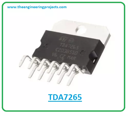
TDA7265 is a +25-watt class AB dual audio power stereo amplifier. This multi-watt package IC is carefully designed for high-quality audio power amplification applications. This device receives a low-input audio signal and amplifies it into a high-quality audio output.
I suggest you buckle up as I will detail the complete introduction to TDA7265 covering datasheet, pinout, features, and applications. Let’s jump right in.
Introduction to TDA7265
- TDA7265 is a +25-watt class AB dual audio power stereo amplifier that is mainly employed in audio amplifiers and woofer amplifiers.
- This device gets a low-input audio signal and converts it into a high-output audio signal.
- This chip features output short circuit protection and comes with a mute-enabled pin.
- Only a few components are required to put this device into working condition.
- Total power dissipation is 30W which is the amount of energy released during the working of this device.
- It comes with an operating voltage range of ±5 to ±25V.
- The operating temperature range is -20°C to +85°C while the storage temperature range is -40°C to +150°C.

TDA7265 Datasheet
Before you apply this component to your electrical project, it’s wise to scan through the datasheet of the device that comes with the main characteristics of the component. Click the link below and download the datasheet of TDA7265.
Additional circuit configurations are available in the datasheet of this chip. You can use any configuration to put this chip in working condition.
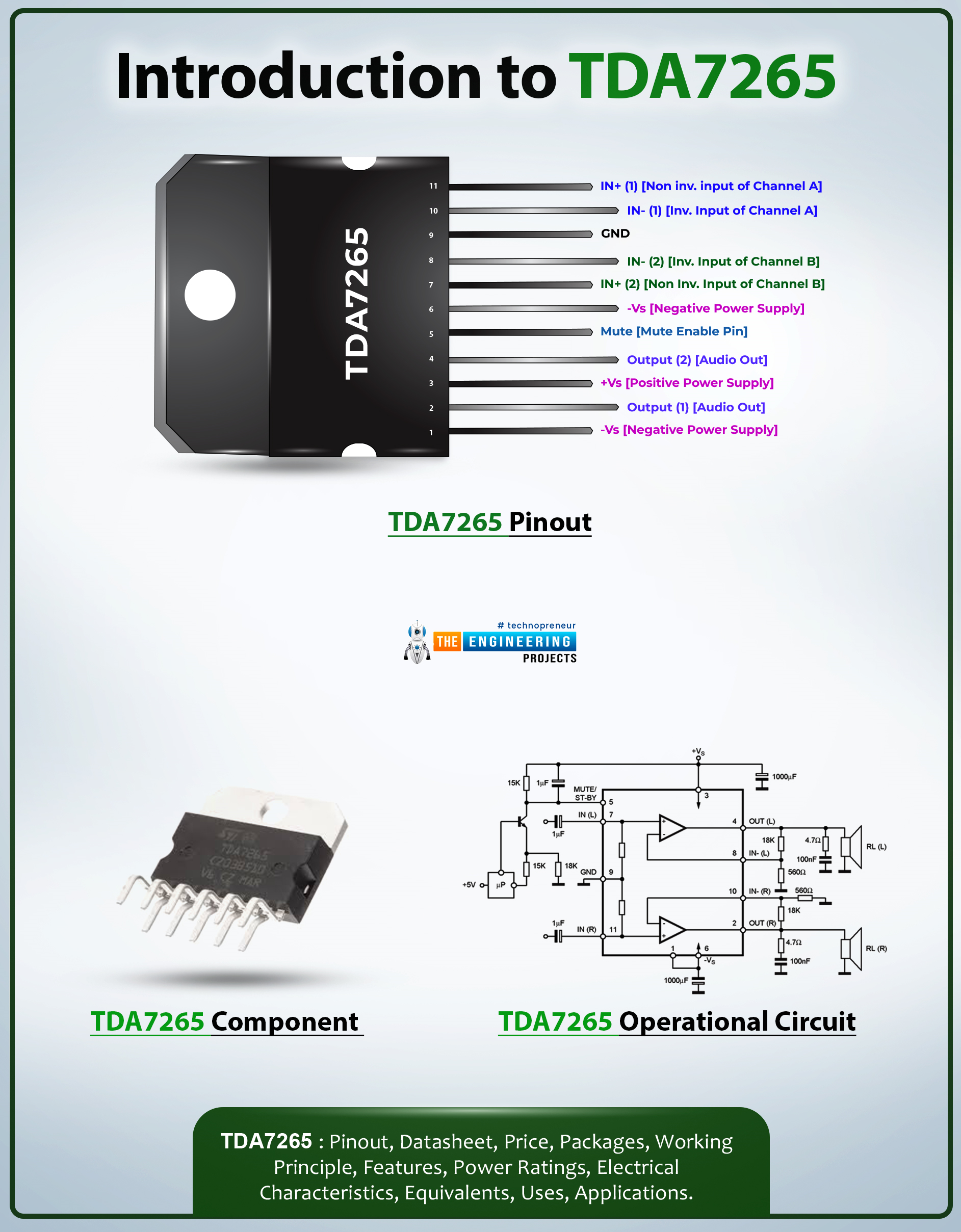
TDA7265 Pinout
The TDA7265 incorporates 11 pins on the device. The following figure shows the pinout diagram of TDA7265.
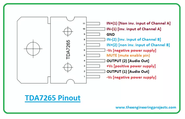
The table below demonstrates the pin name and pin description of each pin on the board.
| Pin Description of TDA7265 | ||||
|---|---|---|---|---|
| Pin No. | Pin Description | Pin Name | ||
| 1 | A negative power supply is connected to this pin | -Vs | ||
| 2 | This pin receives the amplified output of channel A | OUTPUT 1 | ||
| 3 | A positive power supply is connected to this pin | +Vs | ||
| 4 | This pin receives the amplified output of channel B | OUTPUT 2 | ||
| 5 | This pin is triggered low to disable the audio output | MUTE | ||
| 6 | A negative power supply is connected to this pin | -Vs | ||
| 7 | A non-inverting input of channel B amplifier | IN+(2) | ||
| 8 | Inverting input of channel B amplifier | IN-(2) | ||
| 9 | This pin is connected to the ground | GND | ||
| 10 | Inverting input of channel A amplifier | IN-(1) | ||
| 11 | A non-inverting input of channel A amplifier | IN+(1) | ||
TDA7265 Features
The following are the main features of TDA7265.
- Comes with a wide operating supply voltage range
- Available with High output power : 25 + 25 W @ RL = 8 ?, Vs = ± 20V
- Features output short circuit protection
- Comes with a mute enable pin
- Incorporates thermal overload protection
- A few components are required to put the amplifier in working condition
- Stand-by feature (low Iq)
- Total power dissipation = 30W
- Split supply
- Maximum supply voltage = ±25V
- Operating voltage range = ±5 to ±25V
- Repetitive current allowed to draw through each output Max = 4.5A
- Storage Temperature = -40°C to +150°C
- Operating temperature = -20°C to +85°C
- No pop at turn-on/off
TDA7265 Operational Circuit
The following figure shows the operational circuit diagram of TDA7265. You need to connect the components as shown in the figure below. Doing this will put your amplifier in working condition.
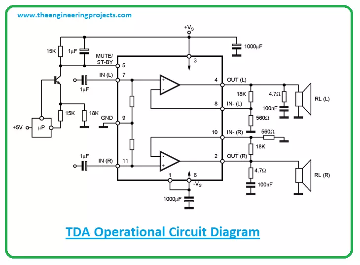
- Two power supplies are used to power up this circuit one with the negative voltage V- and the other with the positive voltage V+.
- Pin no. 11 of this chip is given with the audio input signal for channel B and the resulting amplified output is heard through the right speaker. The Pin no. 07 of this chip is given with the audio input signal for channel A and the resulting amplified output is heard through the left speaker.
- A positive voltage supply source is used to power up the TDA7265 chip while the separate control unit is used to trigger the mute pin low. The two amplified outputs behave as a dual supply operation.
TDA7265 Applications
The TDA7265 is used in the following applications.- Employed in stereo TV sets
- Incorporated in woofer amplifiers
- Used in audio power amplifiers
- Used in music players
- Used in student and hobby projects
- Employed in guitar amplifiers
- Used in Hi-Fi music centers
That’s all for today. I hope you’ve enjoyed reading this article. If you’re unsure or have any questions, you can ask me in the section below. I’d love to help you the best way I can. Feel free to share your valuable suggestions and feedback around the content we share, so we keep producing quality content customized to your exact needs and requirements. Thank you for reading the post.