CA3130 MOSFET BiMOS Op-Amp Datasheet, Pinout, Features & Applications


Hi Everyone! Hope you’re well today. I welcome you on board. In this post today, I’ll walk you through the Introduction to CA3130.
The CA3130 is a BiMOS Operational Amplifier that comes with MOSFET at the output. The term BiMOS suggests that it projects the advantage of both Bipolar and CMOS op-amp technology.
This IC comes with high bandwidth due to bipolar op-amps and consumes less current due to CMOS op-amp, making it a perfect fit for mobile jammers and voltage follower circuits.
I suggest you read this post all the way through as I’ll detail the complete Introduction to CA3130 covering datasheet, pinout, features, and applications. Let’s get started.
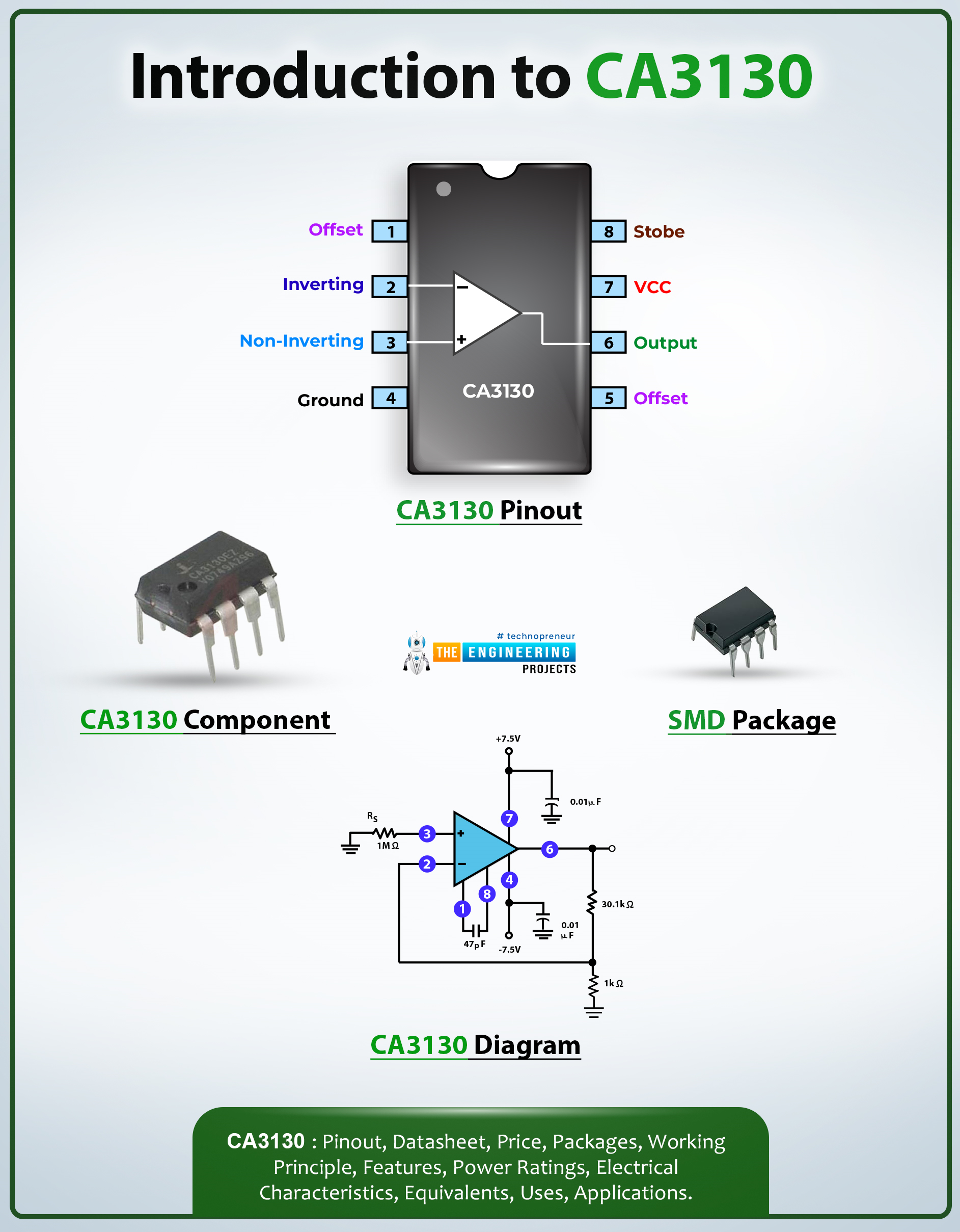
Introduction to CA3130
- The CA3130 is a BiMOS Operational Amplifier that contains MOSFET at the output. This chip consumes less current and features high bandwidth.
- This device has high input impedance due to MOSFETs which implies that when an output voltage of the sensor is connected to the inverting or non-inverting terminals of the op-amp, the output voltage from the sensor will not be disturbed since the op-amp will not act as a load to the sensor.
- If you’re looking for a device with high input impedance, less power consumption, and high bandwidth, this chip might be the answer.
- CA3130 is an eight-terminal electronic IC that comes with a Common Mode Rejection Ration (CMRR) of 80dB.
- It is widely used in frequency generators and noise detectors.
- The input terminal current of this device is 1mA and the supply current is 10mA.
- The CA3130 features inverting and non-inverting pins like other op-amps. If the voltage at the non-inverting pin is high, the output across the inverting pin will be high, otherwise, it will be low.
- Pins 1 & 5 are offset null pins used to nullify the offset produced when two input pins are combined. When the input pins of the op-amp are combined with each other, the voltage at the output should be zero. But no operational amplifier is ideally perfect. So when two inputs are combined together, it results in the offset. The offset null pins are used to null that effect.
- Pin 8 is called Strobe that is mainly used to turn off the output stage. It is also employed for phase compensation in comparators.
CA3130 Datasheet
Before you incorporate this device into your electrical project, it’s wise to go through the datasheet of the device that features the main characteristics of the component. Click the link below and download the datasheet of CA3130.CA3130 Pinout
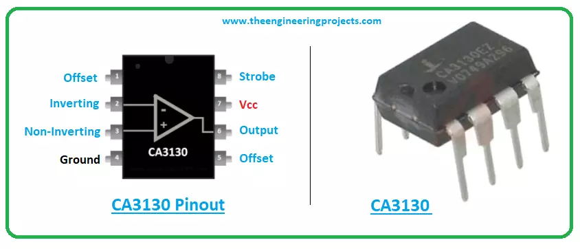
The following figure shows the pinout diagram of CA3130.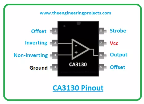
| Pin Description of CA3130 | ||||
|---|---|---|---|---|
| Pin No. | Pin Description | Pin Name | ||
| 1,5 | When the input pins of the op-amp are combined with each other, the voltage at the output should be zero. But no operational amplifier is ideally perfect. So when two inputs are combined together, it results in the offset. The offset null pins are used to null that effect. | Offset Null Pins | ||
| 2 | The Inverting pin is also given a fixed voltage which is compared with the (IN+) | Inverting Input (IN-) | ||
| 3 | The Non-Inverting Pin of the comparator gives a variable voltage to compare | Non-Inverting Input (IN+) | ||
| 4 | This pin is connected to the ground of the system (Negative voltage can also be used) | Ground (VCC-) | ||
| 6 | This is the output pin of the op-amp | Output | ||
| 7 | This VCC pin offers the operating voltage for the Op-Amp. For CA3130 it is up to +16V | VCC+ | ||
| 8 | Allows you to turn off the output stage | Strobe | ||
CA3130 Features
- Op-amp laced with MOSFET at the output
- Input Terminal current = 1mA
- Wide power supply Range i.e. for single supply – 5V to 16V and for dual supply – ±2.5V to ±8V
- Sink current Max. = 20mA
- Source current Max. = 22mA
- Output Voltage Max. = 13.3V
- Supply current = 10mA
- Common Mode Rejection Ration (CMRR) = 80dB
CA3130 Alternatives
The following are the alternatives to CA3130.- LM311
- LM324
- LM358
- LM741
- LM339
CA3130 Applications
The CA3130 is used in the following applications.- Incorporated in DAC circuits
- Used in voltage follower circuits
- Employed in mobile jammers
- Employed in Oscillator circuits
- Used in frequency generator/distorter
- Used in Peak Signal/Noise detectors
That’s all for today. Hope you find this article helpful. If you have any questions, you can pop your comment in the section below. I’d love to help you the best way I can. Feel free to share your valuable feedback and suggestions around the content we share so we keep coming back with quality content customized to your exact needs and requirements. Thank you for reading the article.