Hello seekers! I hope you all are doing great. Today, we are interested to learn about a basic and one of the most crucial topics in the field of electronics that is, the difference between active and passive components. Knowing the difference between these two is not only fruitful for beginners but also helps to understand the output and nature of electrical and electronic devices throughout the circuit design process.While designing electrical or electronic circuits, it is crucial to get the best components. There are different features that affect the performance of these tiny components, including material, type, manufacturing techniques, etc. It's a good practice to get the components from a trusted source, and I suggest you buy them from PCBWay.
This is one of the most trusted sour ...
Hello everyone. Today is a great day that we are going to put our focus on another type of PCB. So far in the previous articles, we have looked at high speed, metalcore, high density interconnect and the ceramic types of PCBs. In this article, we are going to introduce another type of PCB that might find great use in your day-to-day interaction with the printed circuit boards. it is very important for a designer to take note of how PCBs have evolved and how they have become an important aspect in the design of successful electronic devices. It has become hardly difficult to come across any time of an electronic device that does not involve the use of printed circuit boards.
In PCB boards you come across LEDs fixed in them, and due to the evolving w ...
Specifying heavy copper—boards with 4 oz/ft² or thicker layers—is rarely done for light-duty applications. It is a decision driven by a specific thermal management challenge: moving massive current through a limited space without compromising the board's integrity. Whether building EV motor controllers or renewable energy inverters, the physics remains the same.
Here is the catch: Standard online PCB calculators often fail to capture the reality of heavy copper.
Most designers instinctively grab a free calculator or a generic IPC chart, plug in the current, and size the trace. While effective for standard 1 oz logic boards, these tools rely on linear assumptions that break down at 4 oz, 10 oz, or heavier weights. Designing for high-power applications requires understanding how these boar ...
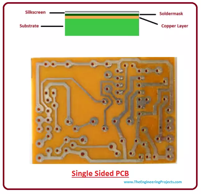
Hey Fellas! Welcome to our website. Today, I am going to share the 2nd chapter in the PCB learning series, where we will discuss Single-sided PCB in detail. In Single-sided PCB, the copper layer is present only on one side of the
PCB and the other side is used for incorporating electronic components. This type of PCB is used in simple circuits with low component density. The conductive tracks in single-sided PCB can't cross each other because of a single copper layer.Let's dive in and explore more,
I'll try to cover every aspect related to Single-sided PCB:
Single Sided PCBSingle-sided PCB, also termed as single-layer PCB(though there's a slight difference), is the simplest type of PCB where the copper layer is present only on one side of the b ...
The digital industry is evolving day by day. Today, computers and phones are no longer heavy. They are sleek, powerful, and very light. Actually, some smartphones are more powerful than laptops. All this is possible because of the miniaturization of the electronic gadgets' printed circuit boards (PCBs).
Printed Circuit Boards or PCBs are categorized into several types based on design specifications, manufacturing processes, and application requirements. They are used in various sectors such as automotive, medical, defense, and other areas, you can learn more information at PadPCB.
Before you select a PCB, there are several factors you need to consider. Moreover, it is essential to seek advice from professionals. Although there are several types of ...
Hi Guys! Hope you’re well today. I welcome you on board. In this post today, I’ll walk you through 10 must-have tools for PCB designing.
If you’re a hobbyist or working as a professional electronics engineer in some company, you need to execute electrical projects on and off. And needless to say, designing a PCB is a crucial part of an electrical project. Scores of tools are available online and it’s difficult for you to choose the right pick for your project.
10 Must-Have Tools for PCB Designing
The reason I have pulled together the 10 best software tools that you can use to design the printed circuit board. Some are better than others. Plus, some are free to use and a few of them are paid software, I’ll describe the main features of both of the ...
Hi Guys! Hope you’re well today. I welcome you on board. In this post, I’ll walk you through How to Optimize a PCB Panel Layout.
PCB panels are used in the manufacturing process to produce PCBs in large numbers. This not only reduces the overall cost but also makes the manufacturing process more efficient and reliable. PCB panelization is a manufacturing technique where multiple PCB designs are replicated on a single large board called a PCB panel. Then these individual boards are removed and depanelized from the panel to install them in the final product.
The number of panels is directly related to the overall manufacturing cost. To produce more panels, more cost will be required. However, it also depends on the shape of the board. If ...
Hi Friends! Happy to see you around. Thank you for clicking this read. In this post today, I’ll document a detailed guide on the PCB fabrication process.
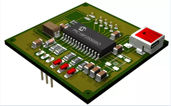
PCB is commonly used in modern electronics. If you uncover the TV set and have a look inside, you’ll find a printed circuit board, electrically connecting components on the board. There are copper traces incorporated on the board to electrically connect the components and provide the current flow from one part to another.
These printed boards make devices precise and compact that are capable of doing more functions than the devices where the end to end wiring is used.
Circuit boards are divided into three main types. Let’s discuss each type one by one so you can better understand the structure ...
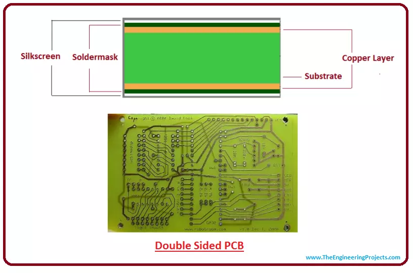
Hey Fellas! I hope you are enjoying your life. Today, I am going to share the 3rd chapter in the PCB learning series. In the last tutorial, we discussed Single-sided PCB in detail and today, we will have a look at the double-sided PCB. In double-sided PCB, the conductive copper layer is present on both sides of the board, unlike single-sided PCB where we have a conductive layer on a single side of the PCB. Thus, we can place electronic components on both sides of the double-sided board and normally use SMD components.Let's jump in and explore more about double-sided PCB:Double Sided PCBDouble Sided PCB is a type of PCB that has conductive copper layers on both sides of the board.
Simply put, double-sided PCB comes with two-sided traces or paths ...
To understand this section, we must know a little history. The history of the development of printed circuits is not as old as that of the industrial revolution, around 1950 is when the first PCBs began to be commercialized, however, in the early 1900s it was when the first attempts at PCB designs emerged.
The human being had the need to have electrical equipment that had a reduced size, before this the search began to replace the complex and extensive cable connections with electronic components.
It was on March 2, 1925, that Charles Ducas first filed a patent that included creating an electrical path directly on an insulating surface.
Technology has advanced and electronics are not left behind, as can be seen in the previous image, the first pr ...