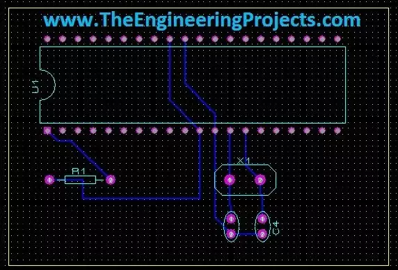
Hello friends! Today we will move from a circuit diagram to a printed circuit board using Proteus ARES. We will use a small PIC16F877A circuit so that placement, connectivity, and routing remain easy to follow. The same sequence of decisions applies when you later design a larger board. Proteus schematic capture describes which component pins belong to each electrical net. PCB layout turns those connections into physical pads and copper tracks. A completed route is useful only when the footprint, pin mapping, power connections, and manufacturing rules are also correct. We will follow the original illustrated workflow: prepare the schematic, transfer its connectivity, define the board edge, place components, and route the board. We will then add the checks needed before sending a design for ...
Hello friends! In this guide, we will learn how to use Proteus ISIS and ARES, starting with a simple circuit and gradually moving toward microcontroller simulations and PCB design. I have kept the original tutorial collection so that you can follow a lesson in detail whenever you reach that stage. Our goal is to understand the complete development process. We will draw a circuit, calculate what it should do, simulate its behavior, examine signals with instruments and then prepare a physical board layout. Each stage answers a different question, so a successful simulation is one step in the process rather than the final proof of a finished product. If you are new to Proteus, follow the sections in order. If you already use it, choose the topic you need from the linked lessons. Some screensh ...