Introduction to BC558

Hello Everyone! Happy to see you here. I welcome you on board. In this post today, I’ll be discussing the Introduction to BC558. BC558 is a bipolar junction transistor used for amplification and switching purposes. It belongs to the PNP transistor family and is available in a TO-92 package. It contains collector current 100mA, indicating it can drive load under 100mA. I've previously detailed the Introduction to BC640 & BC327. I suggest you read this entire post as I will cover a complete introduction to BC558 explaining pinout, working, power ratings, physical dimensions, datasheet, and applications of BC558.   Let’s jump right in. Continue reading.

Introduction to BC558

  • BC558 is a PNP bipolar junction transistor mainly used for switching and amplification purpose.
  • It is made up of three terminals called collector, base, and emitter. All these terminals are different in terms of size, functions, and doping concentrations.
  • The small current change at the base side is used to induce large current change across other terminals. This phenomenon is used for amplification purposes.
  • BC558 is composed of three layers where one is an n-doped layer and others are p-doped layers. The n-doped layer is sandwiched between two p-doped layers.
  • Both electrons and holes play a crucial rule for the transistor conductivity because here in the case of PNP transistor holes are majority carriers in contrast to NPN transistors where electrons are majority carriers.
  • BC558 is also known as a current-controlled device where small current at the base terminal produces a large current change across the remaining terminals.
  • This PNP transistor encompasses amplification factors ranging from 110 to 800. This factor actually predicts the amplification capability of the transistor. Simply put, it defines the capacity of the transistor it can amplify the input signal.
  • BC558 is composed of silicon material and comes in a TO-92 package.
  • The peak collector current is recorded 200mA that makes it a suitable pick for the amplification purpose.

BC558 Datasheet

While working with the electronic component, it’s wise to look at the datasheet that helps you better understand the main characteristic of the component. Click below to download the datasheet of BC558.

BC558 Pinout

BC558 contains three pins named:
  • 1: Collector
  • 2: Base
  • 3: Emitter
As this is a PNP transistor, here current flows from emitter to collector as opposed to NPN transistors where current flows from the collector to emitter.
  • And in both cases, the base terminal is the component that plays a vital role in the overall transistor action.
The following figure shows the pinout of BC558.
  • In this case of PNP transistor, the base terminal controls the number of holes in contrast to the NPN transistor where it controls the number of electrons.
  • And base terminal is negative in PNP transistors where it's positive in NPN transistors.

BC558 Working Principle

  • When there is no current at the base side, both emitter and collector will be closed and the transistor is turned ON, indicating the forward-biased mode of the transistor.
  • And when there is current at the base terminal both emitter and collector will remain opened indicating reverse biased mode of the transistor.
  • The base terminal controls the conductivity of the transistor while the emitter terminal carries the whole current of the transistor.
  • The emitter terminal is highly doped as compared to the other two terminals. The base is negative while both emitter and collector are positive.

BC558 Power Ratings

The following table represents the absolute maximum ratings of the BC558 transistors.
Absolute Maximum Ratings BC558
No. Rating Symbol Value Unit
1 Collector-Emitter Voltage Vce 80 V
2 Collector-Base Voltage Vcb 80 V
3 Emitter-Base Voltage Veb 5 V
4 Collector Current Ic 100 mA
5 Collector Peak Current Icm 200 mA
6 Power Dissipation Ptot 500 mW
7 Storage Temperature Tstg 150 C
  • These are the stress ratings. Before you install this component in your project, make sure these ratings don’t exceed the recommended ratings, else they can severely affect the overall working of the component and in the worst cases, can damage the entire project.
  • Plus, if these ratings are applied for an extended time, the device reliability can be severely damaged.

Difference between PNP and NPN transistors

  • Both transistors almost operate similarly with few exceptions. The voltage polarities and current directions will be reversed.
  • In NPN transistor current flows from collector to emitter and from emitter to collector in case of PNP transistor. And holes are the majority charge carriers in PNP transistors and electrons are major charge carriers in the NPN transistors.
  • And in both cases, the base terminal is responsible for the transistor conductivity i.e. it controls the number of electrons in case of NPN transistor and the number of holes in the case of PNP transistors.
  • It is important to mention NPN are preferred over PNP transistors for amplification purpose because the mobility of electrons is far better and quicker than the movement of holes in PNP transistors.
  • In some cases, however, both are incorporated into a single project to attain amplification.

BC558 Alternatives

The following are a few alternatives to the BC558 transistor.
  • TIP127
  • BC157
  • 2N3906
  • BC556
  • BD140
  • 2SA1943
  • S8550
  • TIP42
Before you incorporate these alternatives into your projects, pay careful heed to the pinout of these alternative transistors, as it’s possible the pinout of the alternatives may differ from the BC558 pinout.

BC558 Applications

The following are some applications of BC558:
  • Used for amplification and switching purposes.
  • Used to control motor.
  • Employed for impedance buffering.
  • Employed to drive loads under 100mA.
  • Incorporated in robotics and instrumentation projects.
  • Used in H- Bridge circuits and current mirror circuits.
  • Used for constructing Astable bistable and Bistable multivibrators.
  • Used in comparator and oscillator circuits.

BC558 Physical dimensions

The following figure shows the physical dimensions of the BC558 transistor. I hope you understand what is BC558 transistor and why it is used for. If you are unsure or have any question in your mind, you can leave your comment in the section below, I’ll help you out with the best of my knowledge. Feel free to keep us updated with your valuable suggestions and feedback, they prove handy and help us create quality work as per your requirements. Thank you for reading this article.

Introduction to BC559

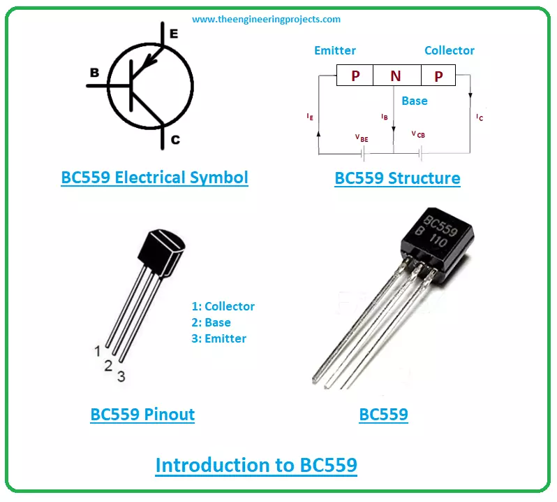
Hi Guys! Hope this finds you well. I welcome you on board. Thank you for clicking this read. In this post today, I’ll be explaining the Introduction to BC559. BC559 is a bipolar junction transistor used to drive loads under 100mA. It falls under the family of PNP transistors and is mainly known as a current-controlled device. Where small current at one terminal is used to drive large current change at the remaining two terminals. Read this post all the way through, as I’ll be touching pinout, working, datasheet, physical dimensions, power ratings, and applications of a BC559 transistor. Let’s get started.

Introduction to BC559

  • BC559 is a PNP bipolar junction transistor mainly employed for amplification and switching applications.
  • It is composed of silicon material and comes in TO-92 packaging. Based on the nature of applications and electronic projects, these transistors are also manufactured in TO-18 configuration.
  • BC559 carries three terminals that are emitter, base, and collector. All these terminals are used for external connection with the circuit.
  • There are three layers inside the PNP BC559 transistor where one n-doped layer stands between two p-doped layers. Here N layer represents the base terminal that is negative and the remaining two terminals are positive.
  • The base terminal is still considered as the main terminal responsible for transistor action.
  • Here base terminal controls the number of holes in contrast to the NPN transistor where the base is positive and controls the number of electrons.
  • The emitter terminal emits the holes which are then collected by the collector terminal.

BC559 Datasheet

The datasheet gives you an overview of the main characteristics of the component. You can check the datasheet of this tiny component by clicking the link below.

BC559 Pinout

BC559 is incorporated with three terminals named:
  • 1: Collector
  • 2: Base
  • 3: Emitter
The following figure represents BC559 pinout.
  • Each terminal carries different doping concentrations and functionality as compared to the remaining two terminals. The emitter side is highly doped in contrast to the other two terminals.

BC559 Working Principle

  • The working principle is simple and straight forward. When there is no current present at the base side, the transistor is turned ON and both emitter and collector are forward biased.
  • And when current flows from the base terminal, the transistor is turned OFF and both emitter and collector terminals will be reverse biased.
  • Though both electrons and holes contribute to conductivity, holes are major carriers in the case of this PNP transistor as opposed to NPN transistors where electrons are major carriers.
  • It is important to note that NPN is preferred over PNP transistors for amplification purposes because the mobility of electrons is far better than the mobility of holes.

BC559 Power Ratings

The table given below contains the absolute maximum ratings of the BC559.
Absolute Maximum Ratings BC559
No. Rating Symbol Value Unit
1 Collector-Emitter Voltage Vce 30 V
2 Collector-Base Voltage Vcb 30 V
3 Emitter-Base Voltage Veb 5 V
4 Collector Current Ic 100 mA
5 Power Dissipation Pd 625 mW
6 DC Current Gain hfe 120 to 800
7 Storage Temperature Tstg -55 to 150 C
  • Both collector-emitter and collector-base voltage is 30V while emitter-base voltage is 5V indicating the only 5V is required to bias the transistor and start the transistor action.
  • The collector current is 100mA means it can support loads under 100mA. Total device dissipation is 625mW and storage junction temperature is -55 to 155 C.
  • You need to be very careful while taking these readings into consideration. If ratings exceed the desired ratings, they can terribly affect the device.
  • And make sure these ratings you don’t apply for more than the required time, else they hurt the device reliability.

Difference between PNP and NPN Transistors

  • Both transistors almost operate in a similar fashion i.e. base is the main terminal responsible for transistor action in both cases and emitter contains the entire current of the transistor.
  • And the emitter terminal is highly doped as compared to other terminals in both cases.
  • There are, however, some exceptions. The voltage polarities and current directions are reversed in both cases. Current flows from emitter to collector in case of PNP transistors while it moves from collector to emitter in case of NPN transistor.
  • The base terminal is negative in PNP transistor while it’s positive in the case of NPN transistor. It acts as a control valve.
  • Recall NPN transistors are preferred over PNP transistors for amplification purposes because the mobility of electrons is better than the mobility of holes.
  • While base terminal controls the electrons in the case of NPN transistors and it controls the holes in the case of PNP transistors.
  • It is important to note that both NPN and PNP transistors are interchangeable given that if a bipolar transistor is composed of two back-to-back diodes with the base terminal being the common terminal.
 

BC559 Alternatives

Following transistors can be used as alternatives to BC559.
  • BC859 (SOT-23)
  • BC858 (SOT-23)
  • BC859W (SOT-323)
  • BC858W (SOT-323)
While you aim to incorporate these alternatives into your project, check the pinout of the alternatives as it’s likely the pinout of the BC559 might differ from the pinout of the alternatives.
  • Be on the safe side and do your due diligence before starting the project.
Complementary NPN transistors of BC559 are BC546 & BC548.

BC559 Applications

BC559 is used in the following applications.
  • Finds applications in current mirror circuits.
  • Used in H- Bridge circuits.
  • Used for constructing Astable bistable multivibrators.
  • Used to drive loads under 100mA.
  • Finds application in comparator and oscillator circuits.
  • Employed for switching and amplification purpose.
  • Incorporated for impedance buffering.
 

BC559 Physical dimensions

BC559 comes in weight approx. 0.18g. The following figure represents the BC559 physical dimensions, helping you evaluate the space given for your project. That was all about Introduction to BC559 transistor. I hope you find this article useful. If you are unsure or have any question, you can approach me in the section below, I’ll help you the best way I can. You are most welcome to pop your valuable feedback and suggestions in the comment section below, they help us produce quality content. Thank you for reading the post.

Introduction to BC560

Hello Friends! Hope this finds you well. I welcome you to another addition to the introduction series. In this post today, I’ll be discussing the Introduction to BC560.

BC560 is a general-purpose transistor mainly used to drive loads under 100mA as it carries collector current 100mA. It falls under the category of PNP transistors and is mainly used for amplification and switching purposes. I suggest you read this entire post as I’ll detail everything about BC560 transistor covering pinout, working, power ratings, applications, and physical dimensions. Continue reading.

Introduction to BC560

  • BC560 is a PNP transistor mainly used for switching and amplification purpose. It comes with transition frequency 150MHz and junction temperature of 150 C.
  • This PNP transistor contains three pins called emitter, base, and collector. These pins are used for external connections with the electronic circuit. The small current at the base side is used to produce large current change across other terminals.
  • BC560 carries three layers where one is the n-doped layer that represents the base terminal and the other two are p-doped layers that represent emitter and collector respectively. The n-doped layer stands between two p-doped layers.
  • As this is a PNP transistor, here current flows from emitter to collector as opposed to NPN transistor where current flows from collector to emitter.
  • Also, here in PNP transistor holes are majority carriers… even though both electrons and holes play a key role in the conductivity of PNP transistors, here holes are majority carriers in contrast to NPN transistors where electrons are majority carriers.
  • In both cases, however, the base terminal is the main component responsible for the overall electron action. Which is positive in the case of NPN transistor and is negative in the case of PNP transistor.
  • Moreover, all these terminals are different in terms of their functionality and doping concentrations. The emitter side is more doped as compared to the other two terminals.
  • Plus, the emitter terminal contains the overall transistor current. The emitter current is a sum of both collector and base current.

BC560 Datasheet

While scanning the datasheet of the component, you can get a hold of the main characteristics of the component. If you want to download the datasheet of the BC560 transistor, click below.

BC560 Pinout

BC560 carries three main terminals known as: 1: Collector 2: Base 3: Emitter
  • These terminals are used for external connection with the circuit.
  • The following figure shows the pinout of the BC560 transistor.
  • It is wise to pay special heed to the pinout of the transistor before employing it in your project.
  • Installing the component with the wrong configuration can damage the component and thus the entire project.

BC560 Working Principle

  • The working principle of this PNP transistor is almost similar to NPN. In both cases, the base terminal triggers the transistor action.
  • When there is no current available at the base terminal, the transistor is turned ON and both collector and emitter terminals are forward biased.
  • And when current flows from the base side, the transistor is turned OFF, indicating both emitter and collector pins are reverse biased.
  • It is important to note that… even though NPN and PNP transistors are used for amplification purposes, NPN transistors are preferred over PNP transistors since the mobility of electrons is far better and quicker than the mobility of holes.

BC560 Power Ratings

The table below carries the absolute maximum ratings of the BC560.
Absolute Maximum Ratings BC560
No. Rating Symbol Value Unit
1 Collector-Emitter Voltage Vce 45 V
2 Collector-Base Voltage Vcb 50 V
3 Emitter-Base Voltage Veb 5 V
4 Collector Current Ic 100 mA
5 Power Dissipation Pd 625 mW
6 Transition Frequency ft 100 MHz
7 Storage Temperature Tstg -55 to 150 C
  • The collector-emitter and collector-base voltages are 45V & 50V respectively. While emitter-base voltage is 5V that means the only 5V is required to start the transistor action.
  • The transition frequency is 100MHz and junction temperature is 150 C. The collector current is 100mA, projecting it can support loads under 100mA.
  • These are the stress ratings which if exceed the required ratings, can hurt the device. And if you apply these ratings more than the required time they can damage the device reliability.

Difference between PNP and NPN Transistors

  • Both NPN and PNP transistors operate almost in a similar fashion. The base pin is the main terminal that plays a key role in triggering the transistor action in both cases.
  • The emitter side is highly doped and contains the entire current of the transistor.
  • Voltage polarities and current directions create a difference between both NPN and PNP transistors.
  • Current flows from collector to emitter in case of NPN transistor while it flows from emitter to collector in case of PNP transistors. The base is negative in PNP transistor while it’s positive in the case of NPN transistor.
  • Recall, mobility of electrons is better than the mobility of holes, the reason NPN are preferred over PNP for amplification purposes.
  • The base terminal acts as a control value in both cases where it controls the holes in PNP transistor and it controls the electrons in case of NPN transistor.
  • Note that, both PNP and NPN transistors are interchangeable only if a bipolar junction transistor is made up of two back-to-back diodes with the base terminal as the common terminal.
 

BC560 Alternatives

The following are the SMD alternatives of BC560:
  • BC860W (SOT-323)
  • BC857W (SOT-323)
  • BC857 (SOT-23)
  • BC860 (SOT-23)
The complementary NPN to the BC560 transistor is BC550.

BC560 Applications

BC560 can be employed in the following applications.
  • Used in current mirror circuits.
  • Used for switching and amplification purpose.
  • Employed for constructing Astable bistable multivibrators.
  • Employed for impedance buffering.
  • Incorporated to drive loads under 100mA.
  • Finds applications in H- Bridge circuits.
  • Used in comparator and oscillator circuits.

BC560 Physical dimensions

The following figure represents the physical dimensions of the transistor BC560. While getting a hold of these dimensions you can evaluate the space required for your entire electrical project. That’s all for today. I hope you’ve got a clear insight into the Introduction to BC560 transistor. If you have any question, you can pop your query in the section below, I’ll help you the best way I can. You are most welcome to share your valuable feedback and suggestions in the comment section below, they help us produce quality content. Thank you for reading the article.

Introduction to BC517

Hi folks! Hope you’re well today. I welcome you on board. In this post today, I’ll detail the complete Introduction to BC517. BC517 is an NPN bipolar junction transistor made up of silicon material and comes in a TO-92 package. It carries collector-current 1A, projecting it can drive loads under 1A. Total power dissipation is 625mW, indicating it releases power around 625mW while working. Collector-emitter and collector-base voltages are 30 and 40 respectively. The emitter-base voltage is 10V which means it requires only 10V to trigger the electron action inside the transistor. Read this post all the way through as I’ll be documenting pinout, working, power ratings, alternatives, applications, and physical dimensions of transistor BC517. Let’s get started.

Introduction to BC517

  • BC517 is a bipolar junction transistor that belongs to the NPN transistor family. It comes in the TO-92 package and is composed of silicon material.
  • It contains three pins known as collector, base, and emitter. The small input current at the base side is used to produce large current at the remaining two terminals. This phenomenon is used for amplification purposes.
  • BC517 comes with three layers where two are n-doped layers and one is a p-doped layer that stands between the two n-doped layers. The p-doped layer represents the base terminal which is positive while the other two terminals are negative.
  • One important feature that makes this transistor unique is its high amplification factor. It carries the current gain or amplification factor around 30,000.
  • The amplification factor is the capacity of any transistor it can amplify the input current. Simply put, the factor by which the current at the base terminal is amplified at the other two terminals.

BC517 Datasheet

  • Before working with any component, it is wise to get a hold of the datasheet of that component that highlights the main characteristic of the device, helping you better understand the component.
  • Click below to download the datasheet of the transistor BC517.

BC517 Pinout

The BC517 comes with three pins called: 1: Collector 2: Base 3: Emitter The following figure shows the pinout of BC517.
  • These are also called transistor terminals that are mainly used for external connection with the electrical circuit. All these pins are different in terms of functionality and doping concentration.
  • Both base and collector terminals are less doped compared to the emitter terminal. Plus, the emitter terminal carries the 100% transistor current. It is a sum of both base and collector current.

BC517 Pin Configuration

BC517 transistor comes in the following three main configurations: 1: Common emitter configuration 2: Common collector configuration 3: Common base configuration
  • Common emitter configuration carries the suitable voltage and current ratings required for amplification purposes. The reasons this configuration is preferred for amplification over the remaining two configurations.
  • The amplification factor or current gain is an important factor of the transistor that mainly projects the capacity of any transistor it can amplify the current. It is denoted by ß.
  • In BC517, the amplification factor is 30,000 which is far high than other transistors in the market. It is a ratio between output energy and input energy i.e. ratio between collector current and the base current.
  • The current gain is another important factor used to describe the nature of the transistor. It is denoted by a and is known as alpha. It is a ratio between collector current and emitter current. The alpha value is always less than 1, commonly stands from 0.5 to 1.

BC517 Working Principle

  • The base side is the key terminal responsible for the overall transistor action. The base terminal gets biased when a voltage is applied to this terminal.
  • The base terminal acts like an electron valve that controls the number of electrons passing through the base pin. The base terminal operates similarly in the PNP transistor but here it controls the number of holes passing through it.
  • During the amplification process, the small current at the base side is amplified and produced across the other terminals.
  • And when BC517 acts like a switch, it converts the small current available at one side of the transistor into a larger current across the other terminals of the transistor.
  • As this is an NPN transistor, here the base terminal is positive with respect to the emitter side and the emitter voltage is less positive than the collector voltage.
Moreover, the collector terminal is laced with the resistor to limit the flow of current.

BC517 Power Ratings

The following table shows the absolute maximum ratings of transistor BC517.
Absolute Maximum Ratings BC517
No. Rating Symbol Value Unit
1 Collector-Emitter Voltage Vce 30 V
2 Collector-Base Voltage Vcb 40 V
3 Emitter-Base Voltage Veb 10 V
4 Collector Current Ic 1 A
5 Current Gain hfe 30,000
6 Power Dissipation Pd 625 mW
7 Storage Temperature Tstg -55 to 150 C
  • Collector-emitter and collector-base voltages are 30 & 40 respectively. While the emitter-base voltage is 10V i.e. it needs 10V to start the electron action in the transistor.
  • The power dissipation is 625mW and junction temperature varies from -55C to 150C. The collector-current is 1A which means it can drive loads under 1A.
  • Be careful while considering these ratings as ratings above these absolute maximum ratings can adversely affect the performance of the component. Also, don’t apply these ratings for more than the required time, else it might affect the device reliability.

BC517 Alternatives

The PNP complementary to BC517 is BC516.

BC517 Applications

It is used in the following applications.
  • Used for amplification and switching purposes.
  • Used in sensor circuits.
  • Employed as an audio preamplifier and amplifier stages.
  • Can drive loads under 1A.
  • Used in battery chargers.
  • Used in H-bridge and Astable and Bistable multivibrators.
  • Used to control motor.
 

BC517 Physical dimensions

The following diagram shows the physical dimensions of transistor BC517. It will help you identify the space required for your electrical project. That’s all for today. I hope you find this article useful. If you have any queries, you can pop your question in the section below and I’ll try my best to help you the best way I can. Moreover, share your feedback and suggestions in the section below, they help us produce quality work. Thanks for reading this post.

Introduction to BC557

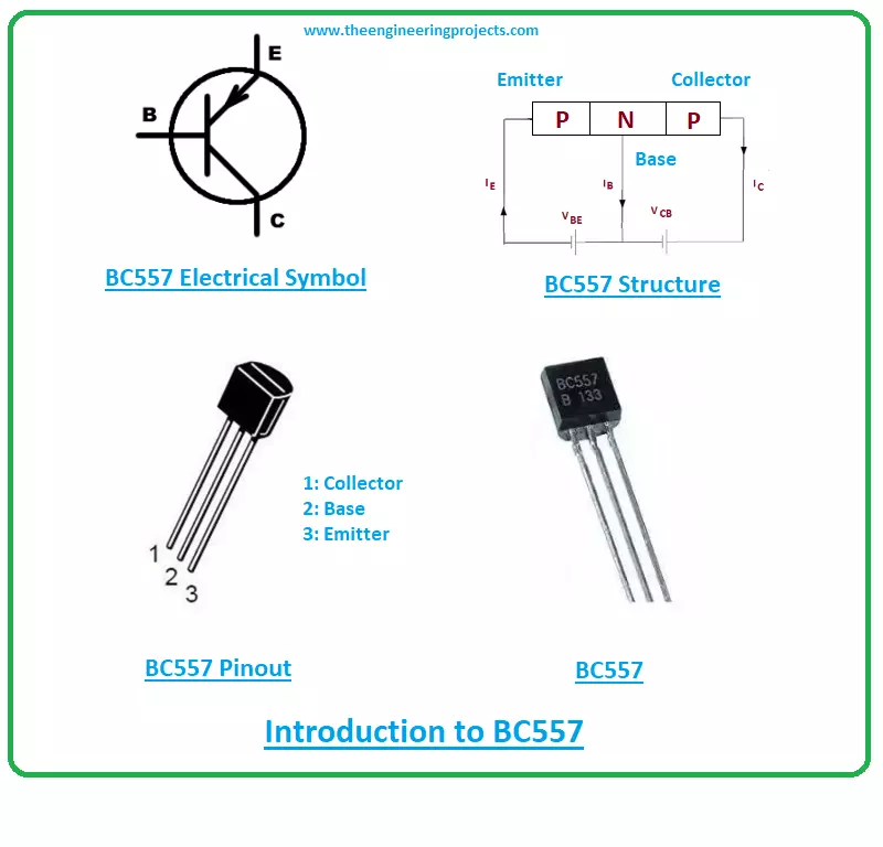
Hi Guys! Hope you’re well. I welcome you on board. Thank you for viewing this read. In this post today, I’ll walk you through the Introduction to BC557. BC557 is a bipolar junction transistor with DC current gain 300. It falls under the category of PNP transistors where one N-doped layer stands between the two P-doped layers. The continuous collector current is 100mA means it can drive load under 100mA. BC557 comes in the TO-92 package and is mainly used for switching and amplification purpose. Before I bore you to tears, let’s dive in and read the complete introduction to BC557 covering datasheet, pinout, working principle, power ratings, physical dimensions, and applications. Continue reading.

Introduction to BC557

  • BC557 is a bipolar junction transistor that falls under the family of PNP transistors.
  • As this is a PNP transistor, there will be no current at the base terminal when the transistor is turned ON and in that case, both emitter and collector will be forward biased.
  • And when voltage is applied at the base terminal, the transistor is turned OFF and both emitter and collector will be reverse biased.
  • It carries three terminals called collector, base, and emitter that are commonly used for external connection with the electronic circuit.
  • All these terminals are different in terms of their size and doping concentration. The emitter is highly doped against both collector and emitter terminals.
  • BC557 contains there layers i.e. two p-doped layers and one n-doped layer. The n-doped layer lies between the two p-doped layers. Here the base terminal is negative while emitter and collector will be positive.
  • The maximum collector current is 100mA indicating we cannot drive loads through the transistor that utilizes more than 100mA current.
  • It is mainly used for amplification purposes. Amplification is the process by which transistor boosts the small input voltage into a large output voltage i.e. small audio signal will be amplified into a large audio signal.

BC557 Datasheet

If you want to download the BC557 datasheet, click the link given below. This will help you understand the main characteristics of the BC557 transistor.

BC557 Pinout

BC557 contains three terminals that are known as:
  • 1: Collector
  • 2: Base
  • 3: Emitter
The following figure shows the pinout of BC557. As this is a PNP transistor, here current flows from emitter to collector and base controls the amount of current. And you may know already, in PNP transistor current flows in through the collector terminal and it drains out through emitter terminal.

BC557 Working Principle

  • In PNP transistor holes are majority carriers as opposed to NPN transistors where electrons are majority carriers. Although holes are majority carriers, the base terminal still plays a key role in the overall action of the transistor.
  • Now holes are emitted from the emitter instead of electrons in the NPN case, and they are collectors by collector terminal.
  • BC557 is called the current controlled device where small current present at the base side is used to control the large current at the remaining terminals.
  • Recall, when the transistor is turned OFF there is a current at the base side and when the transistor is turned ON there is no current present at the base terminal.

BC557 Power Ratings

The following table represents the absolute maximum ratings of BC557.
Absolute Maximum Ratings BC557
No. Rating Symbol Value Unit
1 Collector-Emitter Voltage Vce 45 V
2 Collector-Base Voltage Vcb 50 V
3 Emitter-Base Voltage Veb 5 V
4 Collector Current Ic 100 mA
5 Power Dissipation Ptot 500 mW
6 Peak Collector Current Icm 200 mA
7 Junction Temperature Tstg 150 C
  • The transistor’s amplification capacity is determined by the amplification factor that is a ratio between collector current and emitter current. It exhibits the actual value of the current or input audio signal that the transistor can amplify.
  • Make sure, these ratings remain under control and don’t exceed the recommended values.
  • If values surpass the standard values, they can affect the overall performance of the component, and thus damage the project you’re working on.
  • Also, if these ratings are applied with maximum time, they can ultimately affect device reliability.

Difference between PNP and NPN Transistors

  • Though both transistors are used for amplification and switching purposes, there are few exceptions.
  • In PNP transistor, the current flows from the emitter side to the collector side and in case of NPN transistor current flows from collector to emitter, however, in both cases, the base is the main terminal that controls the amount of current.
  • In PNP transistors, base controls the number of holes and in NPN it controls the number of electrons. As conductivity is carried out by electrons in NPN transistors, they prove handier for amplification purposes compared to PNP transistors because the mobility of electrons is far better and quicker than the movement of holes in PNP transistors.
  • In PNP transistor the base side is negative compared to both emitter and collector while in case of NPN transistor base side is positive compared to remaining terminals.
  • The emitter terminal is both cases is highly doped and carries the 100% current of the transistor.
  • Both NPN and PNP transistors are different in terms of the applied source voltage.
In PNP transistor source voltage is applied across the emitter terminal and in case of NPN transistor it is applied at the collector side.

BC557 Alternatives

BC557 equivalent alternatives are:
  • BC558
  • BD140
  • TIP42
  • BC157
  • S8550
  • 2N3906
  • 2SA1943
  • TIP127
It’s wise to check the pinout of the alternatives before installing them into your electrical project as it’s likely the pinout of the alternatives may differ from the pinout of the BC557. Better do your due diligence beforehand.

BC557 Applications

BC557 is used in the following application:
  • Used for switching and amplification purpose
  • Used to drive load under 100mA
  • Employed in robotics and instrumentation projects
  • Used in motors for controlling current

BC557 Physical dimensions

The following figure shows the physical dimensions of BC557 to help you evaluate the desired space of your electronic project. That’s all about Introduction to BC557. I hope you like this post. If you have anything to add, you can share your insight in the section below. And if you need my technical help regarding the usage of this component in your project, I’m available to help you the best way I can. Thank you for reading this post.
Syed Zain Nasir

I am Syed Zain Nasir, the founder of <a href=https://www.TheEngineeringProjects.com/>The Engineering Projects</a> (TEP). I am a programmer since 2009 before that I just search things, make small projects and now I am sharing my knowledge through this platform.I also work as a freelancer and did many projects related to programming and electrical circuitry. <a href=https://plus.google.com/+SyedZainNasir/>My Google Profile+</a>

Share
Published by
Syed Zain Nasir