In a number of applications where speed, latency, and light detection are critical, silicon has reached the limits of its capabilities. Global shipments of silicon between 2021 and 2025 are expected to total 17,600 million square inches, according to Statista. It is clear from this report that Moore's law has the potential to last at least until 2025. However, it is also critical to identify a suitable silicon substitute.
Future iterations of the machine will be able to learn from and adapt to its environment thanks to technologies like artificial intelligence. Because of this, more potent and flexible computational processes are required. It is more probable that the production of chips will usher in a new computing revolution. The following are a few possible silicon chip substitutes th ...
Hey Guys! I hope you all are doing great. In the previous tutorial, we studied the basics of Semiconductors, where we briefly discussed the PN Junction. Today, we are going to have a detailed overview of PN Junction.
But before getting into the details of PN Junction, we need to first recall a few concepts from the previous lecture:
Semiconductor Basics
As we know, the conductive power of a semiconductor material lies between a conductor and an insulator. So, it can act as a pure conductor as well as a pure insulator, depending on the applied conditions. Semiconductors are divided into two types:
Intrinsic Semiconductor.
Extrinsic Semiconductor.
Intrinsic Semiconductor
A semiconductor in its pure form is called an Intrinsic semiconductor. In this state, the outermost valan ...
Hello Friends, I hope you’re well today. Today, we are going to start a new tutorial series on Semiconductors. In this series, we will discuss the semiconductor components, devices, etc. in detail. We will start from the very basics and will gradually move towards complex concepts. As today's our first tutorial in this series, we will discuss the basics of semiconductors. So, let's get started:
What is a Semiconductor?
A Semiconductor Material is defined by its ability to conduct electricity and its conductive
properties lie between conductor and insulator, normally ranging between 10-6 to 10-4 (Ωm)-1.Under specific conditions, Semiconductors have the ability to act either as a pure conductor or a pure insulator.Examples of Semiconductor materials
are Silicon, Germanium, Gallium A ...
Hi Guys! Hope you’re well. In this post today, we’ll cover What is IGBT? We’ll also discuss IGBT Full Form, Pinout, Meaning, Symbol & Working.BJT (bipolar junction transistor) and MOSFETs (metal-oxide-semiconductor field-effect transistor) are commonly used electronic switches that we’ve already studied in detail. These devices are useful when you deal with low-current applications, however, when it comes to high-current applications, these devices don’t work as expected. This is where the IGBT transistor comes in handy. This device is a combination of both BJT and MOSFET and stands fit for high-current applications.
In this post, we’ll cover What is IGBT in detail.
Let’s get started:1. What is IGBT?
IGBT is a three-pin device made of semiconductor material and is used for fast- ...
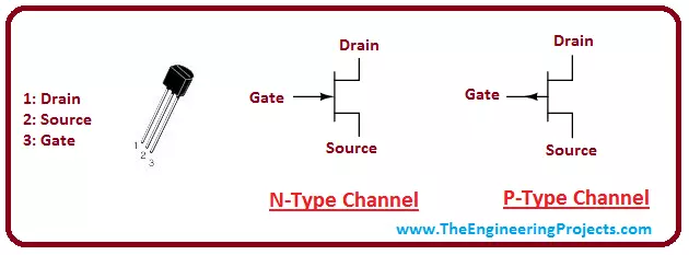
Hello Guys! I hope you are doing great and having fun. I am back to give you a daily dose of knowledge that will enhance your learning skills and put you ahead of others. Today, I am going to give you details on the Introduction to JFET. It is a Junction Field Effect Transistor that consists of three terminals named drain, source and gate. It comes in two configurations called the P-Type channel and the N-Type channel. I'll give you brief details on JFET and try to cover as many aspects as possible. Let's get started:
Introduction to JFET
JFET (Junction Field Effect Transistor) is a uni-polar voltage-controlled device that consists of three terminals called drain, source and gate.
Unlike bipolar junction transistors which are bipolar current-controlled devices in which a small amo ...
Hi Guys! Hope you are doing great. Today, we will have a look at an electronic component named Diode. We will discuss Diode working, Symbol, Applications and characteristics in detail.
A diode is an electronic component, that allows the flow of current in one direction only. It exhibits low resistance in one direction and very high resistance in the opposite direction. Whoever has been a science student, knows about diodes. Although it seems to be a tiny component of a circuit, apparently it is true but it has a lot of complexities or you can say, it's a storm in a teacup.
Diodes are normally used in rectifiers, where they convert AC signals to DC signals. They come with a wide range of applications including power conversion, radio modulation, l ...
Hello, Students here I am present to cover an article on a series of Electronic devices and circuit theory. The foremost article of this series is Ideal diode vs practical diode. I try to elaborate on basic to modern theory related to the diode. This component act as fundamental to many important circuit devices such as rectifiers, transformers, etc. The question which we cover in this article are;
What is a diode?
How a diode is formed? Which methodology manufacturer utilized while the formation of the diode?
What is the concept of doping and PN junction in diode theory?
How does a Diode work?
What type of biasing allows a diode to conduct? Under which situation of biasing diode offers a restriction while conducting?
Upon which cha ...
Hello friends, I hope this article finds you happy, healthy, and content. Today, we are about to discuss one of the most commonly known types of transistors which you might have heard of many times when reading about transistors, the transistor under study is none other than the “Bipolar Junction Transistor’’, also known as BJT . In this article, we will go through the basics of the bipolar junction transistor including its meaning ,definition, types, characteristics, and applications. So, let's get started.
Definition of BJT
A BJT in its full form is written as bipolar junction transistor and we can define it as,
"A bipolar junction transistor is a three-terminal semiconductor device which is made up of two PN junctions within its structure a ...
Hello friends, I hope you all are happy, healthy, and, content. Today, our discussion is all about "Diodes". Whoever has been a science student, knows about diodes. Although it seems to be a tiny component of a circuit, apparently it is true but it has a lot of complexities or you can say, it's a storm in a teacup. You might have read a lot about diodes in physics, in today's discussion we would be moving step by step into the pool of diodes from definition to working of diodes, their types, and then lastly its applications. Let's get started!
Diode Definition
First things first, Let's define diode,
A diode is a basic discreet electronic component made up of semiconductor material, used in electronic circuits, which allows unidirectional c ...
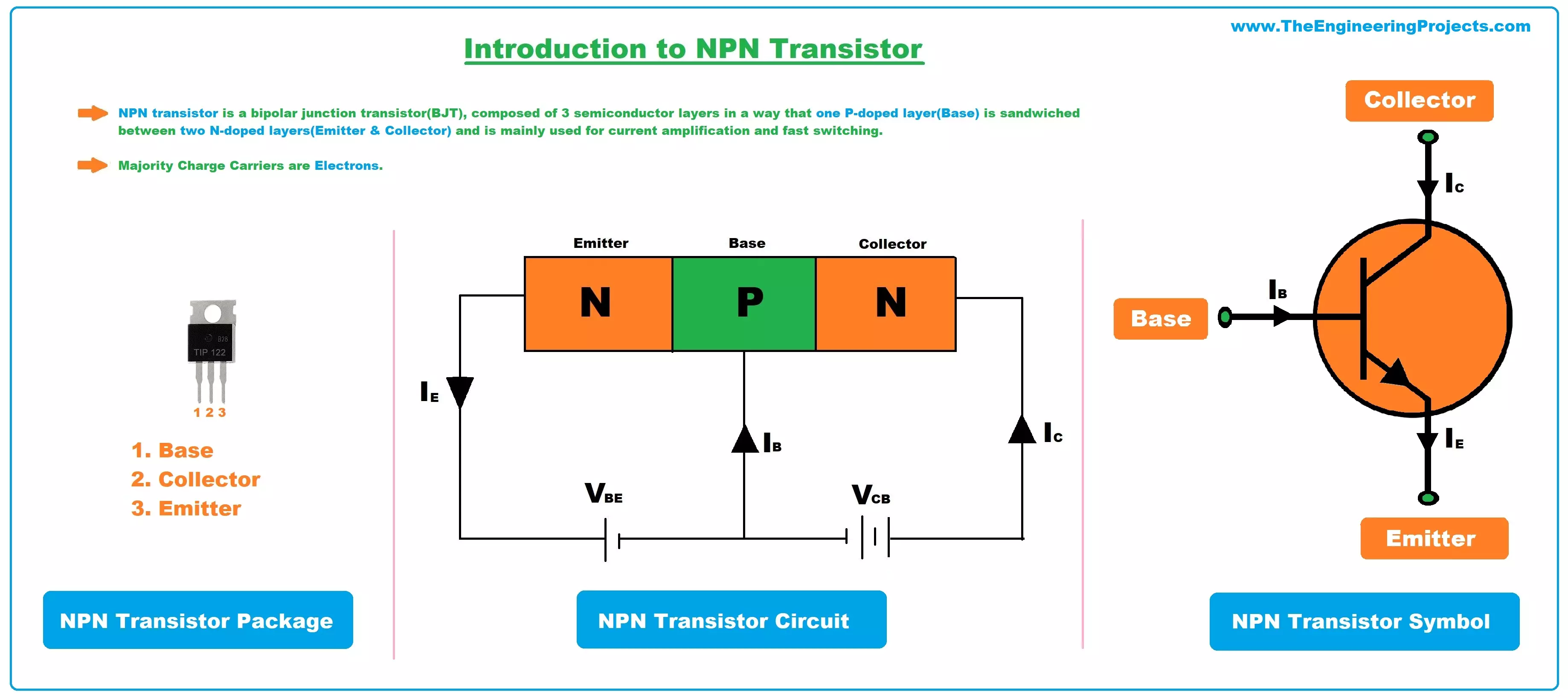
Hello Friends! I hope you are well. Today, I am going to give you a detailed Introduction to NPN transistor. In this tutorial, we'll look at the NPN transistor, how it works, circuit diagram, output characteristics curve, and applications. It is a bipolar junction transistor mainly used for current amplification and switching purposes.
BJTs (Bipolar Junction Transistor) are divided into two types i.e. NPN transistor and PNP transistor. Both transistors are different in terms of their electrical composition and construction, however, both are used for amplification and switching purposes in one way or the other.
What is NPN Transistor?
NPN transistor is a bipolar junction transistor(BJT), composed of 3 semiconductor layers in a way that o ...