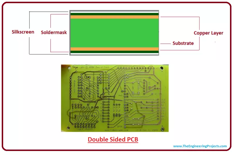
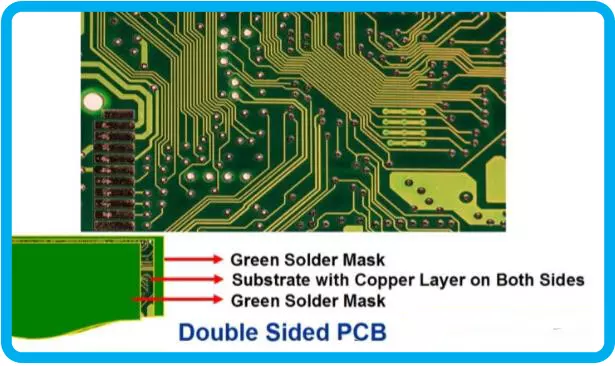
Hey Fellas! I hope you are enjoying your life. Today, I am going to share the 3rd chapter in the PCB learning series. In the last tutorial, we discussed Single-sided PCB in detail and today, we will have a look at the double-sided PCB. In double-sided PCB, the conductive copper layer is present on both sides of the board, unlike single-sided PCB where we have a conductive layer on a single side of the PCB. Thus, we can place electronic components on both sides of the double-sided board and normally use SMD components.Let's jump in and explore more about double-sided PCB:Double Sided PCBDouble Sided PCB is a type of PCB that has conductive copper layers on both sides of the board.
Simply put, double-sided PCB comes with two-sided traces or paths ...
Hello everyone. Today is a great day that we are going to put our focus on another type of PCB. So far in the previous articles, we have looked at high speed, metalcore, high density interconnect and the ceramic types of PCBs. In this article, we are going to introduce another type of PCB that might find great use in your day-to-day interaction with the printed circuit boards. it is very important for a designer to take note of how PCBs have evolved and how they have become an important aspect in the design of successful electronic devices. It has become hardly difficult to come across any time of an electronic device that does not involve the use of printed circuit boards.
In PCB boards you come across LEDs fixed in them, and due to the evolving w ...
Hello! Friends I hope you are all fine. In today's article, we tend to unlock the details on the double sides of PCB which is a type of PCB. It comes with a conductive copper layer on both sides of the board, unlike single layer PCB which has only layer one side of the board. I will try to elaborate on each and everything about double-sided PCB with the best of my effort. So you do not need to move your attention to another source for elaborating this article. In this article, we illustrate the double-layer PCBs, their advantages and disadvantages. We will also study double-layer construction methodology, its applications. In termination, we will discuss the conclusion of today’s article. Let’s start our article by exploring PCB and its main appli ...