Hi Guys! Hope you are doing fine. Today, I am going to give you a detailed Introduction to Transistor. A transistor is a semiconductor device that comes with three terminals, where a small current at one terminal is used to control current at the other terminals. Transistors are mainly used for the amplification of electronic signals. Transistors were first invented by American Physicists John Bardeen in 1947.
Before the inception of transistors, vacuum tubes were used to control the electronic signals. These vacuum tubes come with anode & cathode arrangement and the potential difference across these ends produces the electric current. In the later versions, a filament is added which is used to provide heat to the cathode that directs the electrons towards the anode side. Their complex design, more power consumption set a pathway for the development of the transistors that play an important role in the creation of modern electronic devices.
Before you get ahold of the transistor, I'd highly suggest you read the article on which is the building block of the transistor.
What is Diode?
Before going into the details of the transistor, let's first recall some points from the previous lecture Introduction to Diode:
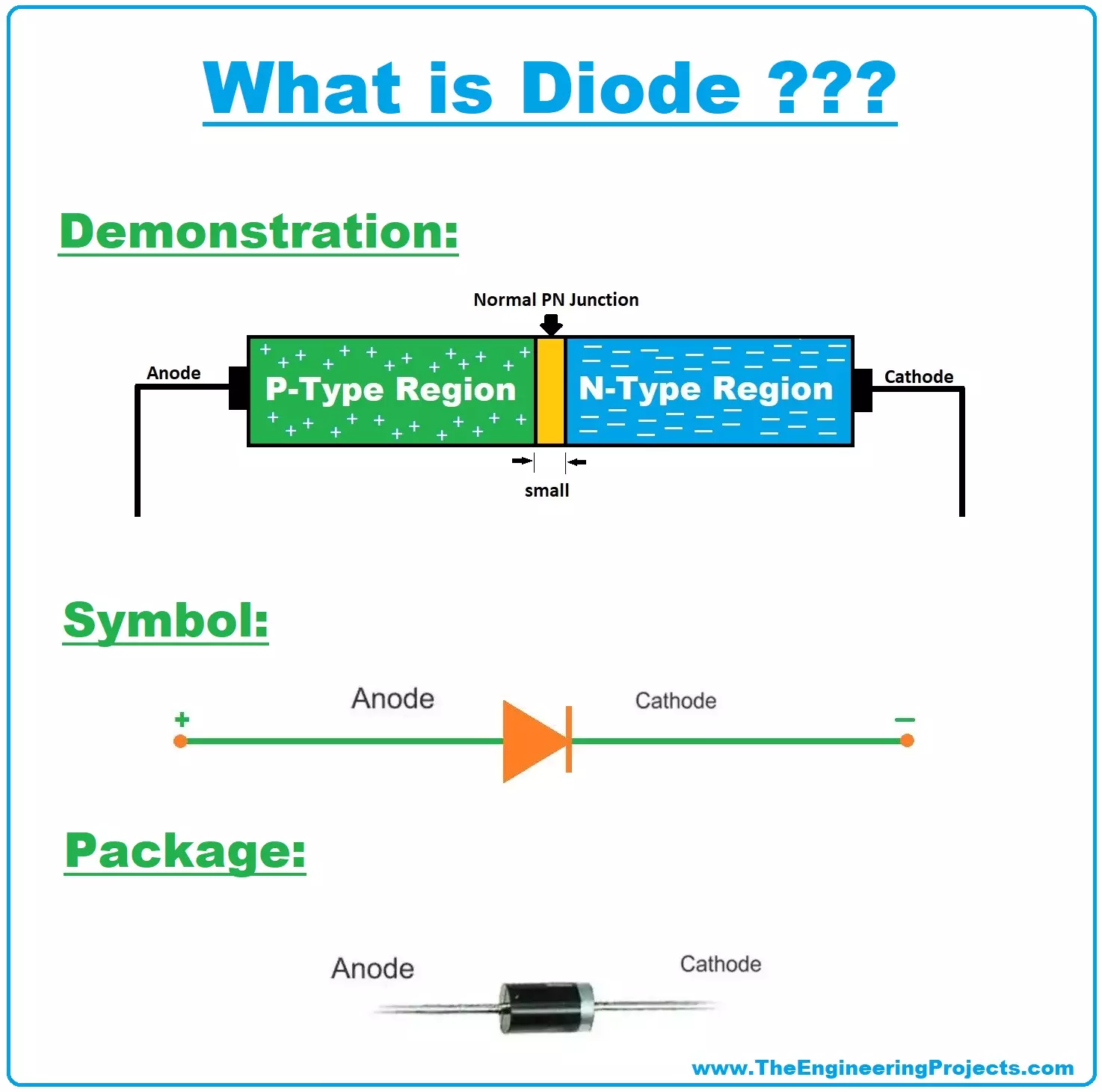
A diode is a semiconductor device, that is developed when two types of semiconductor materials(i.e. N-Type and P-Type) are joined together.
In the construction of the diode, the PN junction is formed by the combination of P-type & N-type material.
Electrons(-ve charge) are major charge carriers in the N-Type material and Holes(+ve charge) are major charge carriers in the P-Type material.
Transistors are formed when an extra layer is added to this PN junction. Transistors come in various types including BJTs, JFETs, MOSFET.
BJTs are the bipolar junction transistors which use two charge carriers i.e. electrons and holes for electrical conduction. And BJTs are the current controlled devices where small current at one terminal is used to control large current at other terminals.
While JFETs are the unipolar devices where conduction is carried out by the movement of only one charge carrier.
Let's dive in and explore what is the main function of a transistor and how it is used for the development of many electronic circuits.
Introduction to Transistor
A transistor is a three-terminal electronic device where small current at one terminal is used to control large current at other terminals. Transistors are mainly used for the amplification of the electronic signals.
Transistor comes with three terminals called emitter, base, and collector which are used for the external connection with electronic circuits.
Transistors were created with the intention of providing cheap electronics. They are available individually, however, most of the time they are packed together in integrated circuits which are then used for the developments of processors, computer memory chips, and complex ICs.
A transistor is a combination of two words i.e. transfer and varistor where each layer comes with an ability to transfer current to other layers when a proper biasing voltage is applied across one of the layers.
Transistor comes with three layers and two PN junctions where an emitter-base junction is forward biased and the collector-base junction is reverse biased.
Most of the transistors are created using silicon and germanium that are less expensive to vacuum tube and require less power to operate.
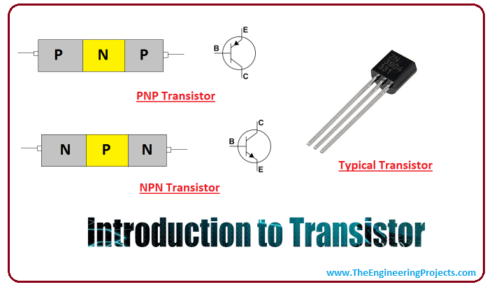
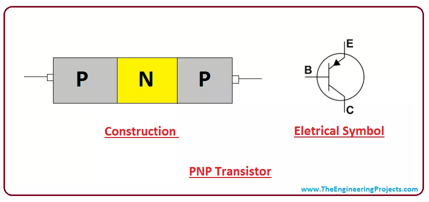
Based on the mobility of major charge carriers, transistors are divided into two types NPN and PNP transistors. Both are different in terms of electrical behaviors and physical construction.
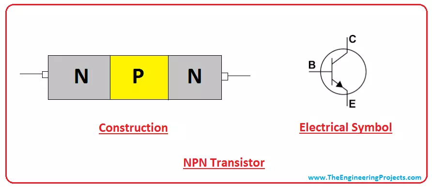
The NPN transistors comes with three layers i.e. two N-doped layers and one P-doped layer. The P-doped layer is sandwiched between two N-doped layers. In NPN transistors, conduction is carried out by both charge carriers i.e. electrons and holes, however, electrons are major charge carriers in NPN transistors.
Similarly, PNP transistors comes with three layers i.e. two P-doped layers and one N-doped layer. The N-doped layer exists between two P-doped layers. Actually, N-doped layer is responsible for triggering transistor action. When a proper bias voltage is applied at the P-doped layer, it draws current which is then used to control large current at other terminals.
Transistors that come in NPN and PNP configurations are nothing but the combinations of two diodes joined back to back.
In NPN transistor current flows from collector to emitter, while in PNP transistor current flows from emitter to collector.
The current directions and voltage polarities are always opposite in both transistors. Suppose, if a current is flowing in a clockwise direction in NPN transistor and comes with positive polarity at the base terminal, it will flow in an anticlockwise direction in PNP transistor where voltage polarity becomes negative.
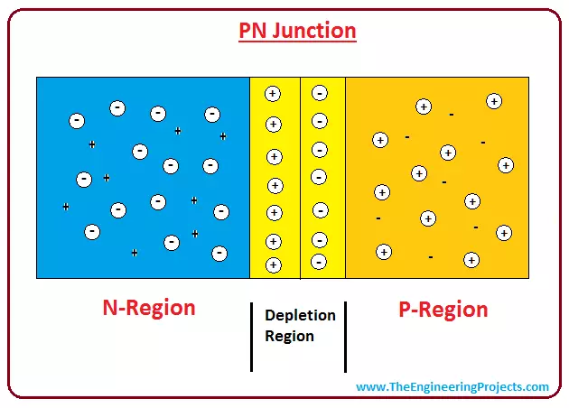
PN junction formed between two semiconductor material is a building block of the transistor. When PN junction is formed, major charge carriers in N-region (electrons) cross the junction and reach the P-region where they recombine with holes. Similarly, major charge carriers in P-region (holes) cross the junction and reach the N-region where they recombine with electrons.
The diffusion of electrons and holes depends on the biasing voltage applied across the junction.
The voltage is said to have forward biased when P-region is connected with positive terminal of the battery and N-region is connected with the negative terminal of the battery.
Under the forward biased condition, holes and electrons can easily cross the junction and maintain a current across the junction. When this diffusion occurs, it will generate the region across the junction which is depleted with major charge carriers. This region is known as depletion region.
As long as the forward biased voltage is applied, current flows across the junction. Diffusion of holes and electrons create an electric field within the junction. This electric field resists the further diffusion of charge carriers.
As said earlier, transistor comes with two PN junctions where one junction is forward biased and other junction is reverse biased.
Modes of Transistor
Transistor comes with different modes of operation. Let's discuss them one by one.
Active Mode
Active mode is used for amplification of the electronic signal where small current at the base terminal is being amplified at the collector terminal.
The base terminal is responsible for the transistor action which controls the number of main charge carriers (electrons in case of NPN transistor and holes in case of PNP transistor) flowing through it and draws a small current when a proper bias voltage is applied.
Cut-Off Mode
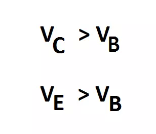
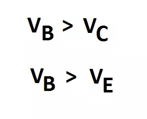
In this mode, transistor works as an open switch and no current flows across the terminals where a base voltage is less than a voltage at other terminals.
Saturation Mode
This mode is considered as an ON switch where current flows freely from collector to emitter.
In this condition, the voltage difference between collector and emitter is zero, and the collector current is restricted by a supply voltage and load resistance.
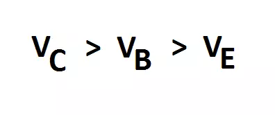
In saturation mode, both junctions are forward biased and base voltage is greater than the voltage at other terminals.
Reverse Active Mode
This mode acts as an active mode with one exception i.e. current direction is reversed.
Current flows from emitter to collector which is proportional to the base current.
The base current is highly influenced by the bias voltage applied at the terminal which then controls large current at other terminals.
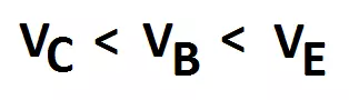
The voltage at the terminals is related in the following way.
Current Gain
Current gain plays an important role in the function of the transistor. Following are two common current gains in a transistor.
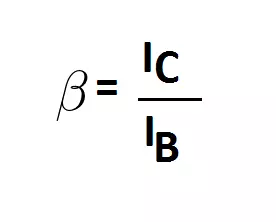
Common-Emitter Current Gain
Common-Emitter current gain is a ratio between collector current and base current.
This is also known as an amplification factor which defines the amount of current being amplified.
It is called beta and denoted by ß. The beta value ranges from 20 to 1000, however, most of the time its value is taken as 50.
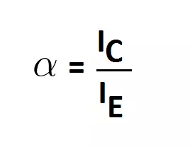
Common-Base Current Gain
Another current gain is common-base current gain which is a ratio between collector current and emitter current.
It is called alpha and denoted by a. The alpha value is taken as unity.
Applications of Transistor
Transistors are mainly used for the amplification of low and high-frequency AC signals.
No current is produced at the collector terminal unless there is a current at the base terminal. This process allows the transistor to work as a switch. The transistor can be turned ON and OFF by controlling the bias voltage at the base terminal.
Based on requirements, a transistor can be made to operate in cut-off or saturation region for switching applications.
Integrated circuits added in the development of the processors are made from transistors.
Used in the development of logarithmic converters and logic gates.
Transistors are widely used in modern electronics especially where signal processing and radio transmission is required.
That's all for today. I hope you have found this article useful. We always keep your demands on the top and develop a content that truly resonates with your field of interest. If you are unsure or have any question, you can ask me in the comment section below. I'd love to help you in any way I can. Thanks for reading the article.