A printed circuit board(PCB) is the most important part of an electronic device. A high-quality PCB is necessary to make a safe and durable device. PCB manufacturers should strive to maintain high quality at a low price. To achieve this goal, some matters should be taken into account.Some key factors affect the prices of PCB manufacturing and assembly. PCB price depends on size, number of layers, quantity, etc. The material that we choose for PCB also affects the cost. The PCB printing process also matters in this regard. For example, some PCB manufacturers print PCBs manually while some control the whole process with CNC machines. Manual PCB printing is cheaper than CNC machine-printed PCBs. PCB manufacturing is a complicated task that needs experience and technology. A trusted PCB partne ...
Hi Friends! Hope you’re well today. I welcome you on board. Happy to see you around. In this post today, I’ll detail PCB Design Online Services for Engineering Students.
PCB designing is a crucial part of making some electrical projects. If you’re a student, you can leverage these services to design PCB online. You can design many PCB layouts for a single layer or multilayer PCB. Moreover, you can test simulation online and see how your design is working that you’re going to execute in real-time.
PCB Design Online Services for Engineering Students
You’ll find a list of online PCB design services. And I can understand, when you’re given a lot of options, it is very difficult to choose the best pick. The reason I have got you covered. In this post, ...
Hi readers! I hope you’re having a great day and exploring something new. If you want a successful PCB, you should have a checklist of rules that are never broken. Today, the topic of our guide is Design Rule Check (DRC) Material and how to avoid common PCB layout mistakes.
In the area of electronic design, the foundation for the construction of all circuits and components is the Printed Circuit Board (PCB). Current device enhancements defined based on size reduction and enhanced complexity require PCB plans to reconcile electrical functionality, mechanical requirements, and assembly potential. A small layout mistake can cause short circuits, faulty connections, or manufacturing delays. This is where Design Rule Check (DRC) comes into play.
DRC is a computer-aided process that becomes pa ...
Greetings and welcome to today’s lecture. It's our 7th tutorial in the PCB learning series. In our previous lectures, we have studied the two main types of PCB i.e. Single-sided and Double-sided PCB. Today is going to be a very interesting and interactive class about Through Hole Technology(THT), which is applied in the process of designing printed circuit boards.A PCB board has a properly designed circuit on it and it's composed of connecting traces/paths and various electronic components. The electronic components are mounted on the board in two different ways i.e. Through-hole and Surface-mount. We will cover Surface-mount in our next lecture and today, we will discuss how to mount components on PCB boards using though-hole technology.So, let's ...
Hi Friends! Happy to see you around. Thank you for clicking this read. In this post today, I’ll document a detailed guide on the PCB fabrication process.
PCB is commonly used in modern electronics. If you uncover the TV set and have a look inside, you’ll find a printed circuit board, electrically connecting components on the board. There are copper traces incorporated on the board to electrically connect the components and provide the current flow from one part to another.
These printed boards make devices precise and compact that are capable of doing more functions than the devices where the end to end wiring is used.
Circuit boards are divided into three main types. Let’s discuss each type one by one so you can better understand the structure ...
Wave soldering is a widely used mass soldering process in the manufacturing of electronics, especially for through-hole elements and intricate technology printed circuit boards. In this method, a PCB is ignored, and a wave of melted solder permits solder joints to form on vulnerable part leads and pads at the same time. While wave soldering is effective and cost-efficient for high-volume manufacture, it is also liable to certain flaws if the method parameters, textiles, or patterns deliberation are not handled carefully.
Wave soldering defects in PCB assembly refer to general soldering flaws, such as spanning, defective solder, voids, and cold joints, that happen during the wave soldering process and can negatively affect the electrical execution, reliability, and long-term endurance of p ...
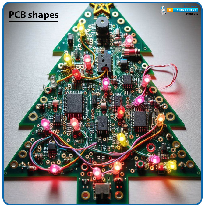
Hello everyone, how are you doing and I hope everybody is doing great. i am going to discuss today the Types of PCB (Printed Circuit Board). Thank you, everyone, for coming back to our website and it means so much. we are grateful for your engagement and most importantly for choosing to educate yourself over anything else in the world.
PCB circuit boards are everywhere and we daily use dozens of circuit boards and interact with them. There is no doubt in saying that the PCB has made our lives easier and advanced. For example, the first thing in the morning your alarm goes off, and wherever you hit snooze, every time you send a signal through its circuit board. And probably the list goes on as you turn the light on off etc.
Let's b ...
JLCPCB (JiaLiChuang Co. Limited) is a worldwide PCB & PCBA Fabrication enterprise. It is a leading company in high-tech manufacturing products specializing in PCB and PCBA production. With over a decade of experience in PCB manufacturing JLCPCB has made over a million customers through online ordering by the customers of PCB manufacturing and PCBA production.
JLCPCB is a professional manufacturer of large-scale manufacturing of PCBs, well equipment, strict management, and superior quality. It deals with the production of all types of PCBs, Stencils, and SMT.
In this article, we are going to discuss widely how the company operates its ordering system of the PCBs by their customers for production through the online booking process.
JLCPCB SMT ...
Hi readers! I hope you are doing well and finding something new. In the high-speed world of electronics, a micrometer of solder paste can make or break your PCB assembly. Today, we will discuss solder paste stencil design and its importance for perfect PCB printing.
Solder paste stencil design is a building block of surface mount technology (SMT) and an important factor in the success of printed circuit board assembly (PCBA). The stencil is an exact template used for depositing solder paste onto PCB pads before the placement of components and soldering. Its design sets the amount of solder paste applied, its location, and how well it picks up from the stencil and gets onto the board. Even slight variations in stencil design can cause major assembly flaws, including solder bridging, inadeq ...
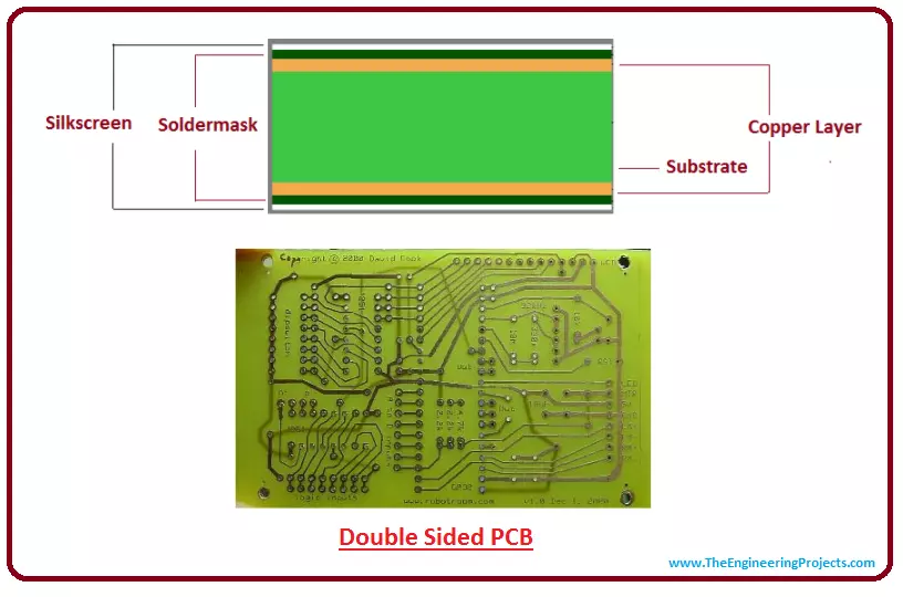
Hey Fellas! I hope you are enjoying your life. Today, I am going to share the 3rd chapter in the PCB learning series. In the last tutorial, we discussed Single-sided PCB in detail and today, we will have a look at the double-sided PCB. In double-sided PCB, the conductive copper layer is present on both sides of the board, unlike single-sided PCB where we have a conductive layer on a single side of the PCB. Thus, we can place electronic components on both sides of the double-sided board and normally use SMD components.Let's jump in and explore more about double-sided PCB:Double Sided PCBDouble Sided PCB is a type of PCB that has conductive copper layers on both sides of the board.
Simply put, double-sided PCB comes with two-sided traces or paths ...