You’ve likely seen this on the bench or in the field. A high-power LED build looks solid during testing but fails prematurely in the real world. The weak link usually isn't the driver or the chip; it’s the board itself. Standard FR4 boards act like thermal blankets, trapping heat exactly where it destroys the junction. If you’re pushing real power—anything beyond a simple indicator—an aluminum PCB isn't a luxury upgrade. It is an engineering necessity to protect your investment from the inevitable thermal load.
The Hidden Heat Problem That Destroys BuildsHigh-power LEDs generate intense heat in a focused surface area. Unlike incandescent bulbs that radiate heat outward, LEDs conduct it down through the package. Here’s the friction point: standard FR ...
Hi innovators! Wishing you the best day. Have you ever waited a couple of weeks for a prototype? Now, these days are gone. Quick-turn PCB redefines the speed of hardware development. In today’s guide, we will discuss how Quick Turn PCB Fabrication helps innovators to launch their product in just a few days.
Quick Turn PCB Fabrication is an accelerated process of manufacturing and delivering printed circuit boards. Quick-turn PCB manufacturing delivers boards in 1-5 business days, significantly faster than the typical multi-week schedule. This quick turnaround plays a vital role in fast prototyping, emergent projects, and applications where speed and innovation are the basis of competitive advantage, such as consumer electronics, automotive, medical devices, and aerospace.
The Quick Turn ...
Hello friends, I hope you all are doing great. In today's tutorial, we are going to have a look at another fabulous fabrication house named WellPCB. I have tried their services recently in an Arduino project, where I need to design a 3-Layer PCB and I was quite satisfied with their services. Before getting into the details, let me point out their strongest point, they have a trained customer service team, which guides you properly & solves all your queries. So, let's have a look at why you should prefer WellPCB for your next PCB order:
A quick review to WellPCB
WellPCB PTY LTD is an Australian company ( daughter company of Uniwell Circuits Co. Ltd. ), focused on the fabrication of PCB, PCBa ( Turnkey ...
Hi Guys! Hope you’re well today. I welcome you on board. Thank you for clicking this read. In this post today, I’ll discuss how to calculate PCB trace width?
The PCB (printed circuit board) is a mechanical layout that electrically connects different components on the board using conductive copper traces that maintained current throughout the circuit board. Different electrical components are placed on the non-conductive substrate which are soldered from the other side of the board. On the non-conductive side of the board copper traces electrically connect these components.
Earlier end-to-end wiring was used in place of PCB boards but now it’s become obsolete. Needless to say, PCB has revolutionized the modern electronics that are precise and com ...
To understand this section, we must know a little history. The history of the development of printed circuits is not as old as that of the industrial revolution, around 1950 is when the first PCBs began to be commercialized, however, in the early 1900s it was when the first attempts at PCB designs emerged.
The human being had the need to have electrical equipment that had a reduced size, before this the search began to replace the complex and extensive cable connections with electronic components.
It was on March 2, 1925, that Charles Ducas first filed a patent that included creating an electrical path directly on an insulating surface.
Technology has advanced and electronics are not left behind, as can be seen in the previous image, the first pr ...
Hello everyone, I hope you all are doing well. In today’s tutorial, we are going to discuss the PCB Etching process, a fundamental step in PCB manufacturing. The PCB Etching process is used to remove the unwanted copper from the PCB surface to reveal the desired circuit pattern.
As we know, a PCB board has a complete copper layer in its raw form. We design our circuit in the software(i.e. Eagle, Altium, Proteus etc.) and place the pattern on the PCB board. This circuit pattern is normally protected by the tin plating, as shown in the below figure:
Now, there’s a need to remove the extra/unwanted copper layer from the PCB board and this process is called the PCB Etching Process. PCB Etching is carried out in various ways and the most commonly used i ...
In the realm of PCB manufacturing, the Gerber file format plays an important role in the design and production processes. Understanding and inspecting these files are crucial to ensuring the accuracy and quality of the printed circuit board (PCB). JLCPCB is a leading PCB fabrication and assembly service provider. Fortunately, it offers an exceptional online tool. It is called the JLCPCB Online Gerber Viewer. It simplifies and enhances the inspection of PCB layouts. In this article, we will discuss the significance of Gerber files. We will explore the reasons for inspection. We will also showcase the powerful functionalities of JLCPCB's Online Gerber Viewer.
What is a Gerber file?
A Gerber file, named after the famous G ...
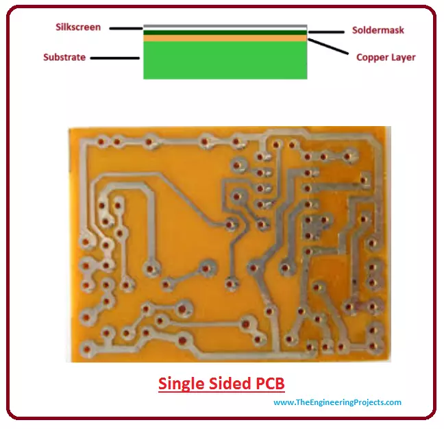
Hey Fellas! Welcome to our website. Today, I am going to share the 2nd chapter in the PCB learning series, where we will discuss Single-sided PCB in detail. In Single-sided PCB, the copper layer is present only on one side of the
PCB and the other side is used for incorporating electronic components. This type of PCB is used in simple circuits with low component density. The conductive tracks in single-sided PCB can't cross each other because of a single copper layer.Let's dive in and explore more,
I'll try to cover every aspect related to Single-sided PCB:
Single Sided PCBSingle-sided PCB, also termed as single-layer PCB(though there's a slight difference), is the simplest type of PCB where the copper layer is present only on one side of the b ...
Solder (or brazing filler metal) serves as a filler metal in the process of brazing. In contemporary manufacturing, welding technology functions as an essential method for uniting electronic components, metal parts, and precise devices. The solder melting temperature has a direct impact on the quality, effectiveness, and suitable situations for welding. From conventional tin-lead alloys to eco-friendly lead-free options, and specialized high-melting-point solders or low-temperature solders, the differences in melting single temperature illustrate a significant interaction among material science, technological needs, and environmental policies.
The Solder Material System
Conventional solder compositions are lead-based solders mainly con ...
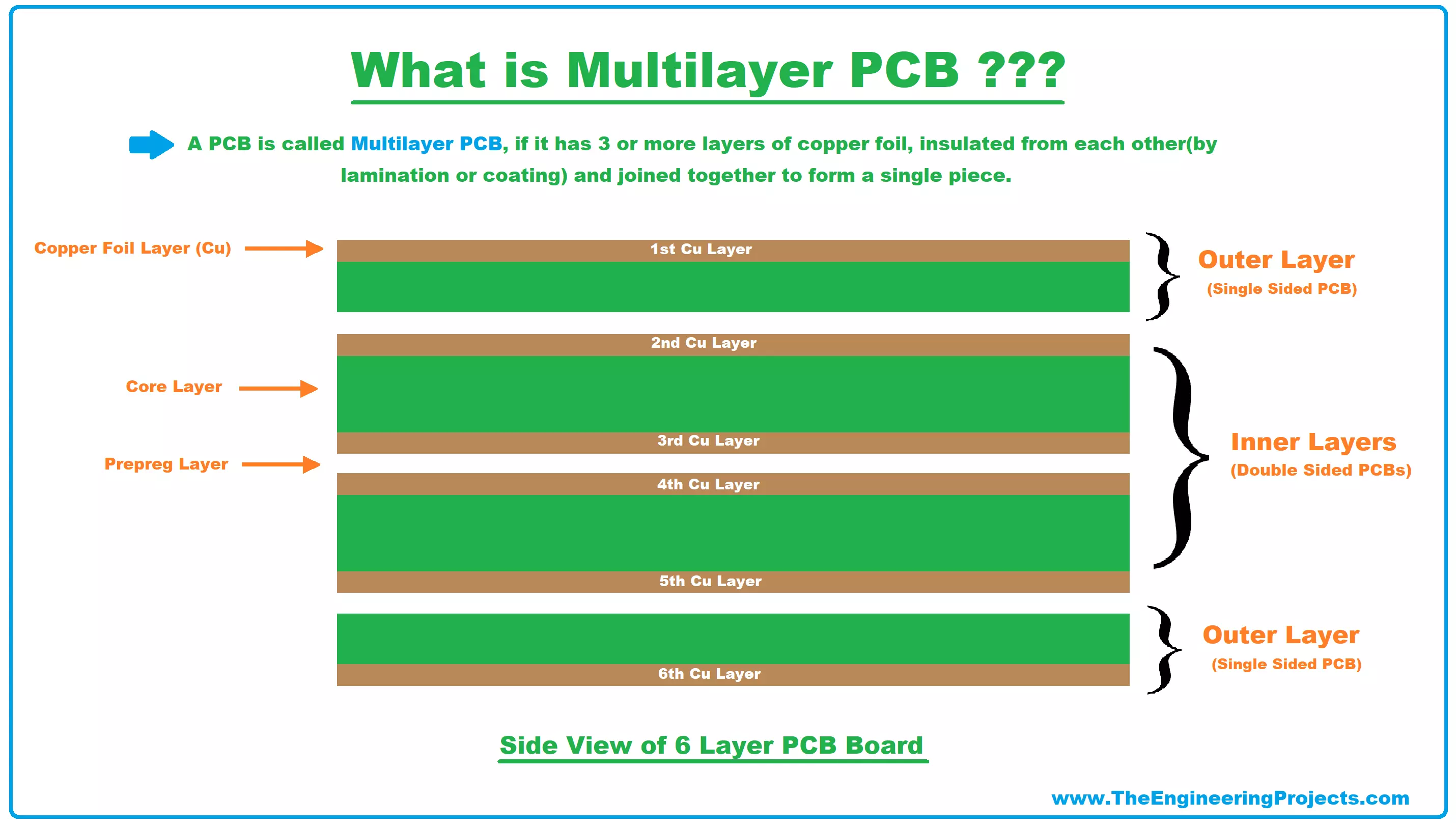
Hello Friends! I hope you all are well. Today, I am going
to share the 15th lecture in the PCB learning series. I am going to give
you a detailed overview of Multilayer PCB,
we will cover what is Multilayer PCB? & why do we need to use it?
We will also discuss its Construction, advantages, disadvantages, etc.
We have seen single-sided PCB
and double-sided PCB
in our previous posts, so go through them first.
Let's first have a look at the definition of PCB: PCB
is an abbreviation of the printed circuit board,
which comes with different copper conductive paths, traces & pads, incorporated on a single board to electrically connect different electronic components.
So, let's get started with What is MultiLayer PCB?
What is Multilayer PCB?
Initiall ...