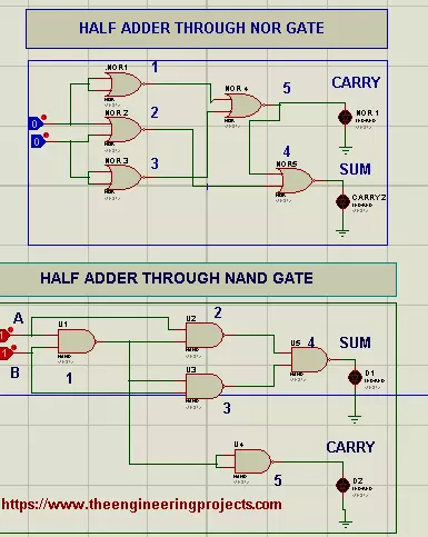
Hello Pupils! I welcome you to The Engineering Projects. I hope you are having a good day. In our previous lecture, we discussed Half-Adder Circuit Designing with XOR and AND logic gates. Today, we are going to design the same circuit using universal logic gates i.e. NOR and NAND gates.We are going to learn the following topics, in today's lecture:
What is Adder?
What is Half Adder?How can We make Half Adder Circuit through NAND Gate?
How can We make Half Adder through just NOR Gate?
Hence without wasting time, Let's find all the Answers.
What is Adder?As we discussed in the last lecture, the DLD Adder is a simple electronic circuit, used to add binary numbers in bit form.There are two types of DLD Adders, named:
Half Adder
Full Adder
In this article, we'll f ...
Hello friends! Welcome to another useful article of The Engineering Projects. I hope you are having a shinning day. Let's add some reproductive information in your day. Today we'll grasp about the establishment skills in Engineering Consultant Firm. Consequently, we'll learn about 6 tremendous ideas for the Establishment an Engineering Consultant.
Starting any business can be difficult. As a matter of fact, some individuals state that around a third of new enterprises fail within the first year of operation. From there, this does not get any easier. These numbers increase to half by the second year of running a business.
This might put you off when you decide to start your engineering consulting firms. However, you can make an engineering consult ...
Hi Mentees! I hope you all are having a Productive Day. In our previous lecture, we discussed the DLD Basic Logic Gates and simulated them in Proteus. Today, we are going to use these standard logic gates and will design another logic gate named NOR Gate and will also simulate it in Proteus.
In this tutorial, we'll learn the following concepts:
What is a NOR Gate?Why NOR is called Universal Gate?
How to derive other Gates through NOR Gate?
Advantages of NOR Gate.
Let's begin the exploration:
What is a NOR Gate?"NOR gate is designed by inverting the output of an OR Gate, so it gives a HIGH output, only when all the inputs are LOW."In simple words, a NOR Gate has an OR Gate followed by the NOT Gate, as shown in the below figure:
...
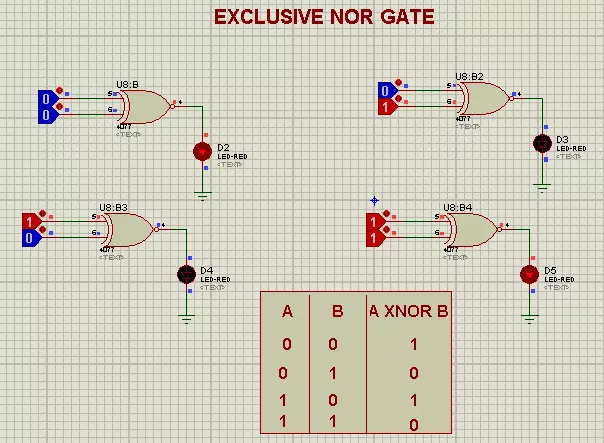
Hello Mentees!, I hope you have a productive day. Welcome to The Engineering Projects. In the previous lecture, we discussed the XOR Logic Gate and designed its circuit using basic logic gates i.e. AND, OR and NOT. Today, I am going to explain another Logic Gate named XNOR Gate in detail.We are going to discuss these concepts in today's lecture:
What are Exclusive NOR Gates
Experimental Proof in Proteus ISIS.
How Truth Table of Exclusive NOR Gate is designed.
How is its Timing Diagram?
Circuit of Exclusive NOR Gate in Proteus Simulation
Applications of Exclusive NOR Gates
XNOR Gate
The exclusive NOR Gate(also called XNOR Gate) simply inverts the output of the XOR Gate(we discussed in the last lecture).So, if we simply place a NOT Gate in front of the XOR Gate, we wi ...
Hi Guys! I welcome you on board. Happy to see you around. In this post today, I’ll walk you through the Introduction to ATmega4809.
The ATmega4809 is a type of microcontroller that belongs to the megaAVR® 0-series. It features an AVR® processor with a clock speed running at up to 20 MHz. It comes with a Flash memory size up to 48 KB, 256 bytes of EEPROM, and 6 KB of SRAM. It is available in 28-, 32-, 40-, or 48-pin packages.
I suggest you buckle up as I’ll detail the complete Introduction to ATmega4809 covering datasheet, pinout, features, power ratings, and applications.
Let’s get started.
Introduction to ATmega4809
The ATmega4809 microcontroller belongs to the megaAVR® 0-series that contains an AVR processor.
The series carries low power ...
Hello Pupils! I welcome you to The Engineering Projects. I hope you are having a good day. In our previous lectures, we simulated almost all the DLD Logic Gates i.e. AND, OR, NOT, NOR, NAND, XOR and XNOR. I hope now you must have a complete understanding of the logic gates and their working.
Now, it's time to have a look at the reason for inventing these logic gates. These DLD logic gates are used to design different numerical modules i.e. adder, subtracter, multiplexer, de-multiplexer, encoder, decoder etc. These arithmetic modules are normally used in electronic products i.e. a simple microcontroller has numerous adders/subtractors for properly calling the registers' addresses.
So, from today onward, we are going to discuss these applications of logic gates one by one. Today, we wi ...
Hello Learners! Welcome to The Engineering Projects. In the previous tutorial, we discussed the first universal gate i.e. NOR Gate and simulated it in Proteus. Today, we are going to focus on the second universal gate i.e. NAND Gate. We will also derive basic logic gates from the NAND gate, to prove its universality.
Today, we'll seek the answers to the following questions:
What is a NAND Gate?What is a Universal Gate?
NAND as a Universal Gate.
NAND Gate as Universal Gate in Proteus ISIS.
Let's get started:
What is a NAND Gate?
A NAND Gate is designed by inverting the output of AND Gate and thus it gives a LOW output when all of its inputs are HIGH, otherwise, it's HGIH.In order to design a NAND gate, simply place a NOT gate in ...
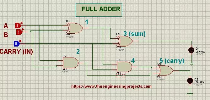
Hello Learners! I hope you are doing great. Welcome to The Engineering Projects. In our previous lecture, we discussed How to design Half Adder with Universal Gates. In today's tutorial, we are going to design Full Adder with Logical Gates.
In today's tutorial, we will learn the complete information about:
What is Adder?
What is Full Adder?
How is the Truth Table of Full Adder?
How can we design Full Adder in Proteus ISIS?
What are the uses of Full Adder?
What is Adder?
Recalling from our previous lectures:The Adders are simple Logical Circuits that take the bits in as the input, sum the bits together and generate the sum and the carry at the output.Adders are present in computer architecture, mainly to control the ...
Hello Learners, hope you are doing well. I am here with a new tutorial. We'll discuss about Junction Field Effect transistors. In this tutorial, we will learn the basic Introduction to JFET nad will also have a look at its practical Implementation and simulation in Proteus.
Basically, Junction Field Effect is a type of transistor, similar to Bipolar Junction Transistors but they have different characteristics due to some reasons as discussed below:
Introduction to JFET
We Define the JFET as:
"Junction Field Effect transistors or simply JFET is the semiconductor ,Voltage Control, three terminal device that is present in both configurations either N channel or P channel."
JFET are named so because the the operation of JFET relies on the Field of th ...
Hi Friends! Happy to see you around. Thank you for clicking this read. In this post today, I’ll document a detailed guide on the PCB fabrication process.
PCB is commonly used in modern electronics. If you uncover the TV set and have a look inside, you’ll find a printed circuit board, electrically connecting components on the board. There are copper traces incorporated on the board to electrically connect the components and provide the current flow from one part to another.
These printed boards make devices precise and compact that are capable of doing more functions than the devices where the end to end wiring is used.
Circuit boards are divided into three main types. Let’s discuss each type one by one so you can better understand the structure ...