Hello Friends! Hope you’re well. Today, I am going to share the 11th chapter in the PCB learning series. In today’s post, I’ll walk you through PCB Panelization, where we will discuss its definition, types, combinations, manufacturing guidelines etc.In PCB companies, CNC machines are used for PCB manufacturing and assembly. These CNC machines are capable of designing PCBs of quite large sizes. But normally, small-sized PCBs are used in electronic products. So, in order to fully utilize the power of CNC machines, PCB design is replicated multiple times(let’s say 10) and this final design is then fed to the CNC machine. This process of manufacturing multiple PCBs on a single board is called PCB Panelization and the final board created is called P ...
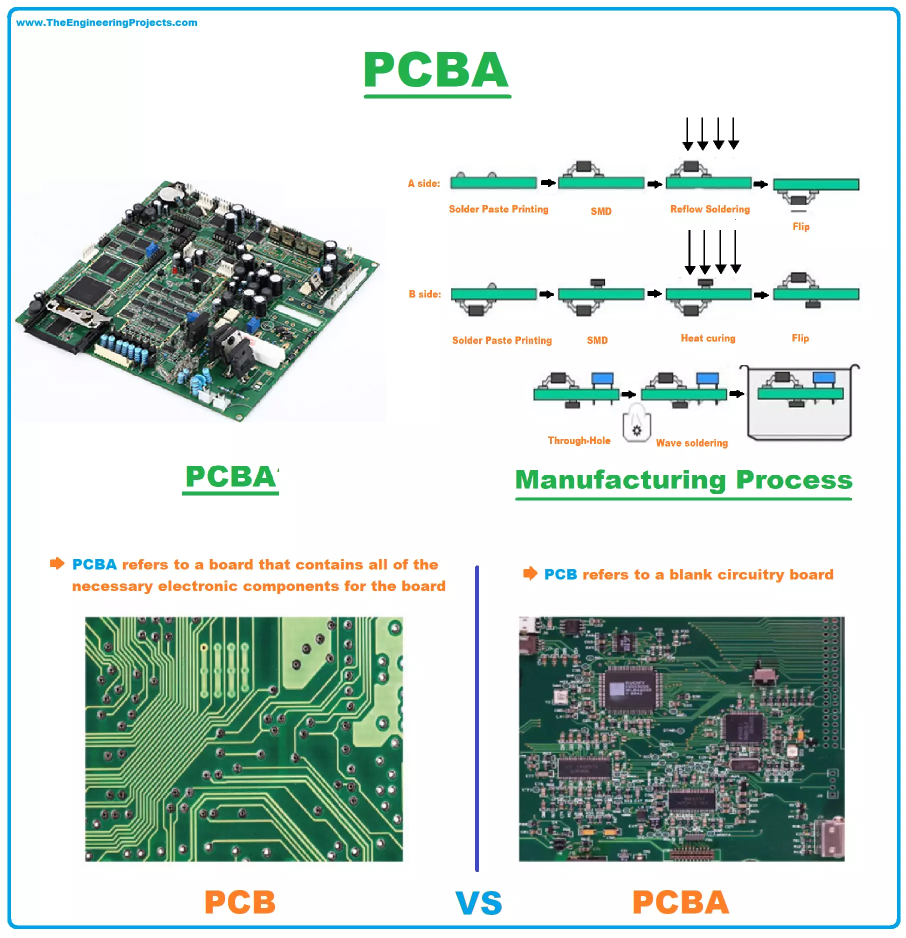
Hey Guys! Hope you’re well. I welcome you on board. In this post today, I’ll walk you through PCBA (Printed Circuit Board Assembly) in detail. It's our 4th tutorial in the PCB learning series.
In the 1st tutorial, we studied printed circuit board(PCB) in detail and learned that PCB provides physical support and electrical connection through conductive copper layers for the electronic components placed on the board. We have seen in our previous tutorials that when we place our PCB order on some PCB fabrication house, they provide us with a PCB board without electronic components. We have to solder the electronic components on the board. But now these PCB companies also offer a service to provide finished PCB boards with electronic components attach ...
Hi Friends! I welcome you on board. Happy to see you around. In this post today, I’ll document a detailed guide on the PCB manufacturing process.
PCB is hands down a crucial part of modern electronics. From cell phones and digital clocks to remote control and television sets, you will find inside a printed circuit board that connects the electrical components through sophisticated layers of copper traces. These electrical copper traces help in the flow of current through the connected components.
Needless to say, PCB has revolutionized the electronics industry. You’ll never find bulky electronics incorporated with scores of wires and electrical components. Nowadays, electronic devices are more compact and sophisticated, cover less space, and ...
Hey Guys! We welcome you on board. Technology evolves every day with the addition of advanced components and devices that make our lives easy. A few years back we were dependent on end-to-end wiring and connectors to electrically connect different electronic components. The inception of PCB substantially removed the need of an end to end wiring and gave an entirely new look to the electronic industry.
In this article, I'll give you a detailed Introduction to Aluminum PCB. It is a type of PCB that uses dielectric thermally conductive and electrically insulated material between the copper layer and aluminum metal. This PCB is a highly effective choice for applications that involve heat dissipation or high temperature. You must have a quick look at M ...
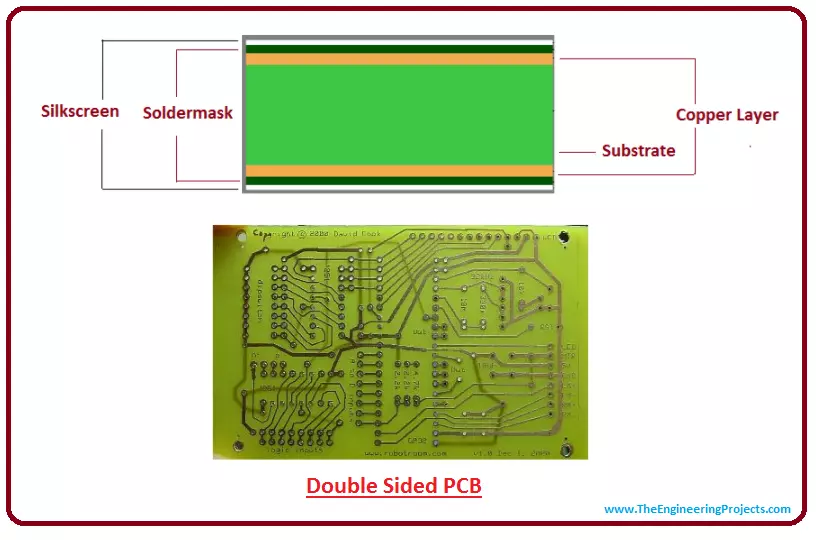
Hey Fellas! I hope you are enjoying your life. Today, I am going to share the 3rd chapter in the PCB learning series. In the last tutorial, we discussed Single-sided PCB in detail and today, we will have a look at the double-sided PCB. In double-sided PCB, the conductive copper layer is present on both sides of the board, unlike single-sided PCB where we have a conductive layer on a single side of the PCB. Thus, we can place electronic components on both sides of the double-sided board and normally use SMD components.Let's jump in and explore more about double-sided PCB:Double Sided PCBDouble Sided PCB is a type of PCB that has conductive copper layers on both sides of the board.
Simply put, double-sided PCB comes with two-sided traces or paths ...
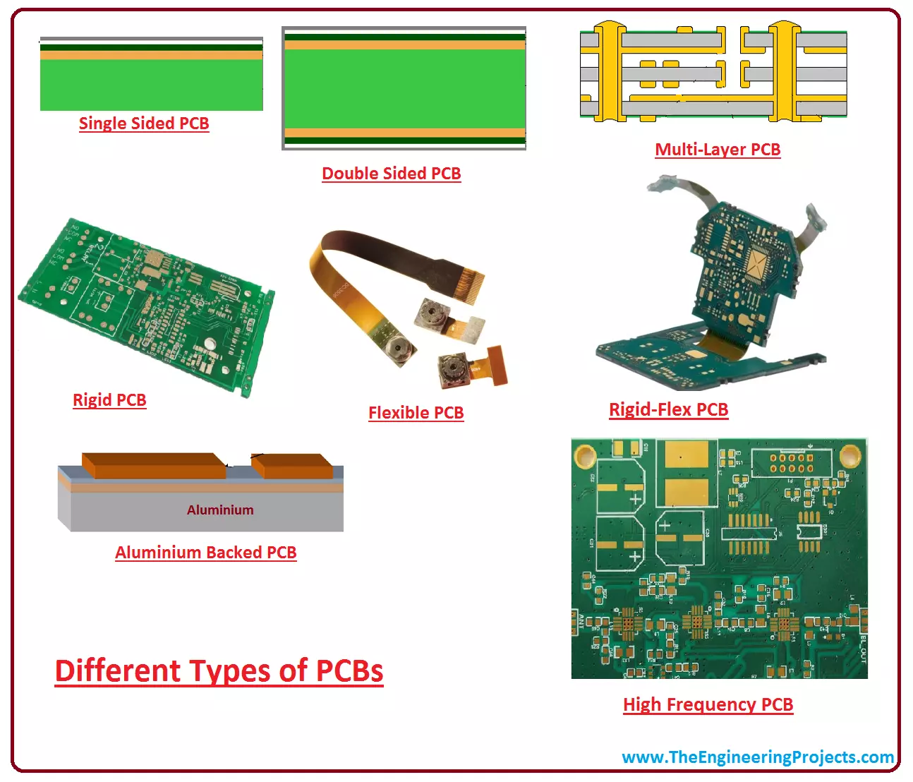
Hello Everyone! I hope you all are doing well. Today, I am going to share the 12th chapter in the PCB learning series. In today's lecture, we will have a look at the Different Types of PCB(Printed Circuit Board). We are familiar with the PCB, it is a printed circuit board that contains traces, lines and paths to electrically connect electronic components. It consists of a substrate on which copper conducting material is laminated for creating an electrical connection between components.Let's dive in and explore these types of PCB boards:
Types of PCB(Printed Circuit Boards)
Following is the list of available types of PCB types. You can choose any PCB based on your requirements:
Single-Layer PCB ...
I remember the first time I handed off a PCB project without thinking hard enough about the assembly process. The board came back looking fine. Then we started testing. Footprint mismatch on a critical power IC. Wrong polarity on an electrolytic cap. Two components missing entirely. Three weeks of schedule gone. The factory had done exactly what we asked them to do. The problem was what we asked for.That experience taught me something most engineering programs never cover. The assembly model you choose matters as much as the circuit design itself. And turnkey PCB assembly is one of those decisions that gets made too casually, too often.What Turnkey PCB Assembly Actually Means
The word turnkey gets used loosely in manufacturing. In PCB assembly it ha ...
Specifying heavy copper—boards with 4 oz/ft² or thicker layers—is rarely done for light-duty applications. It is a decision driven by a specific thermal management challenge: moving massive current through a limited space without compromising the board's integrity. Whether building EV motor controllers or renewable energy inverters, the physics remains the same.
Here is the catch: Standard online PCB calculators often fail to capture the reality of heavy copper.
Most designers instinctively grab a free calculator or a generic IPC chart, plug in the current, and size the trace. While effective for standard 1 oz logic boards, these tools rely on linear assumptions that break down at 4 oz, 10 oz, or heavier weights. Designing for high-power applications requires understanding how these boar ...
You’ve likely seen this on the bench or in the field. A high-power LED build looks solid during testing but fails prematurely in the real world. The weak link usually isn't the driver or the chip; it’s the board itself. Standard FR4 boards act like thermal blankets, trapping heat exactly where it destroys the junction. If you’re pushing real power—anything beyond a simple indicator—an aluminum PCB isn't a luxury upgrade. It is an engineering necessity to protect your investment from the inevitable thermal load.
The Hidden Heat Problem That Destroys BuildsHigh-power LEDs generate intense heat in a focused surface area. Unlike incandescent bulbs that radiate heat outward, LEDs conduct it down through the package. Here’s the friction point: standard FR ...
Wave soldering is a widely used mass soldering process in the manufacturing of electronics, especially for through-hole elements and intricate technology printed circuit boards. In this method, a PCB is ignored, and a wave of melted solder permits solder joints to form on vulnerable part leads and pads at the same time. While wave soldering is effective and cost-efficient for high-volume manufacture, it is also liable to certain flaws if the method parameters, textiles, or patterns deliberation are not handled carefully.
Wave soldering defects in PCB assembly refer to general soldering flaws, such as spanning, defective solder, voids, and cold joints, that happen during the wave soldering process and can negatively affect the electrical execution, reliability, and long-term endurance of p ...